
Thin-BOX metal backgate extremely thin SOI device

a metal backgate and ultra-thin technology, applied in the field of semiconductor devices, can solve the problems of increasing leakage current and variability, reducing the service life of the backgate, so as to prevent metal oxidation during fabrication, improve service life, and reduce the effect of resistan

Inactive Publication Date: 2013-04-30
IBM CORP
View PDF6 Cites 5 Cited by
  • Summary
  • Abstract
  • Description
  • Claims
  • Application Information

AI Technical Summary

Benefits of technology

The invention provides a semiconductor device with a thin layer of nitride to prevent metal oxidation during fabrication. This helps to improve the performance of the device by controlling the short channel and reducing the impact of leakage current on the drain. The device includes nFETs and pFETs with backgate metal, which can be independently biased. Overall, this technology enhances the stability and efficiency of the semiconductor device.

Problems solved by technology

Nevertheless, performance improvement brought up by this type of “classic” scaling, in device dimensions, has recently met obstacles and in some cases even been challenged, when the scaling goes beyond a certain point, by the increase in leakage current and variability that are inevitably associated with the continued reduction in device dimensions.
Shallow junctions are necessary to avoid lateral diffusion of implanted dopants into the channel, since such diffusion disadvantageously contributes to leakage currents and poor breakdown performance.
STI techniques significantly increase the manufacturing cost because the STI process requires a large number of processing steps and apparatus, such as thermal oxidation, silicon nitride chemical vapor deposition (CVD), silicon nitride wet etch, reactive ion etch (RIE), high density plasma (HDP) silicon oxide deposition, wet clean, chemical-mechanical polishing (CMP), and photolithography.
The challenge of this class of transistors is its Vt variation and high extrinsic resistance (Rext).
Since the ETSOI devices are fully depleted, changes in body thickness result in changes in the charge in the body which, by Gauss' law, results in changes in the channel potential, altering the threshold voltage.
As transistors shrink further in dimension, the ability to scale down the gate length of conventional bulk silicon MOSFET diminishes due to SCE.
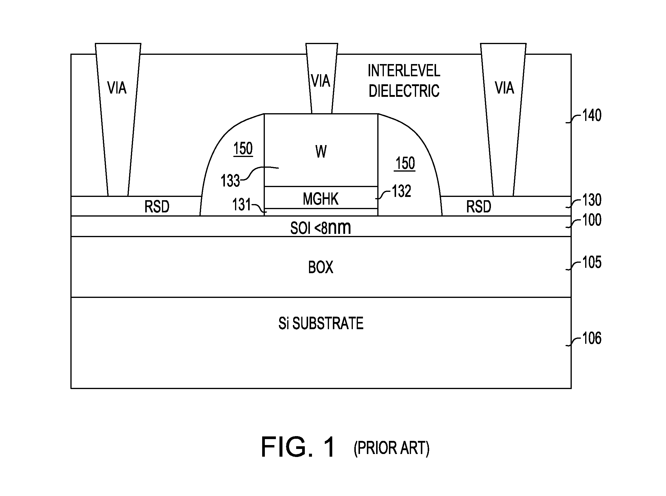
However, the Single Gate FDSOI technology may require a stringent thickness requirement and uniformity control of the thin silicon film on insulator to achieve full depletion.
Additionally, the aforementioned Drain-Induced Virtual Substrate Biasing (DIVSB) effect is another challenge for Single Gate FDSOI technology.
Due to the extremely thin SOI layer 105, the active SD and Extension regions experience create difficulties for dopant implants and activation annealing.
Although implants can be conducted, only partial dopants are activated due to lack of silicon re-crystallization.
The sheet resistance from both active regions is so elevated that its electrostatic performance is severely degraded.
Because halo implant for a good Vt control is not applicable, resulting in a high Vt and device punch-through.

Method used


Image

  • Thin-BOX metal backgate extremely thin SOI device
  • Thin-BOX metal backgate extremely thin SOI device
  • Thin-BOX metal backgate extremely thin SOI device

Examples


Embodiment Construction

[0032]The present invention will now be described in greater detail by referring to the following discussion and drawings that accompany the present application. It is noted that the drawings of the present application are provided for illustrative purposes only and, as such, they are not drawn to scale. In the following description, numerous specific details are set forth, such as particular structures, components and materials, dimensions, processing steps and techniques, in order to provide a thorough understanding of the present invention. However, it will be appreciated by one of ordinary skill in the art that the invention may be practiced without these specific details. In other instances, well-known structures or processing steps have not been described in detail in order to avoid obscuring the invention.

[0033]Moreover, it will be understood that when an element as a layer, region or substrate is referred to as being “on” or “over” another element, it can be directly on the ...


PUM

PropertyMeasurementUnit
thicknessaaaaaaaaaa
thicknessaaaaaaaaaa
thicknessaaaaaaaaaa

Abstract

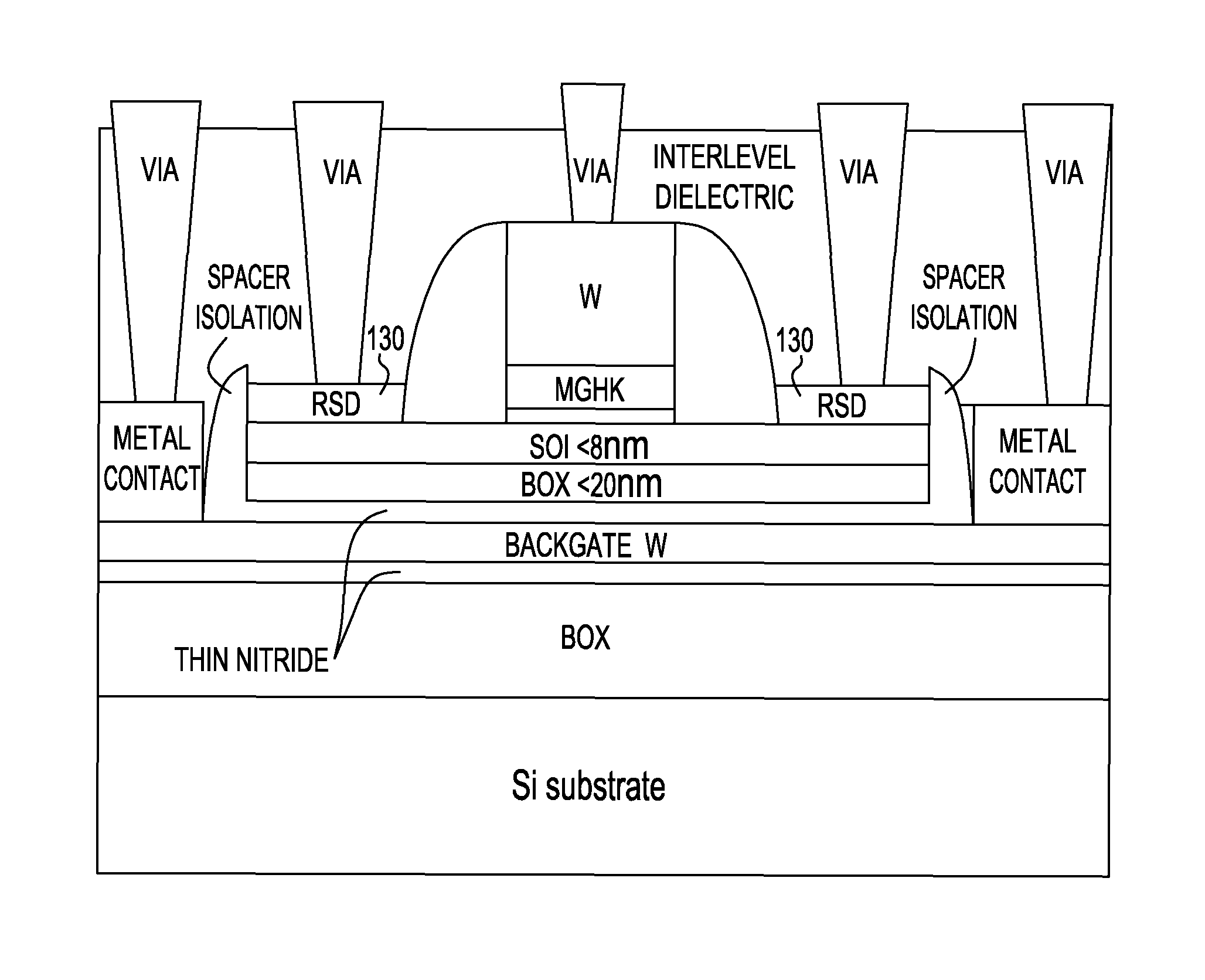
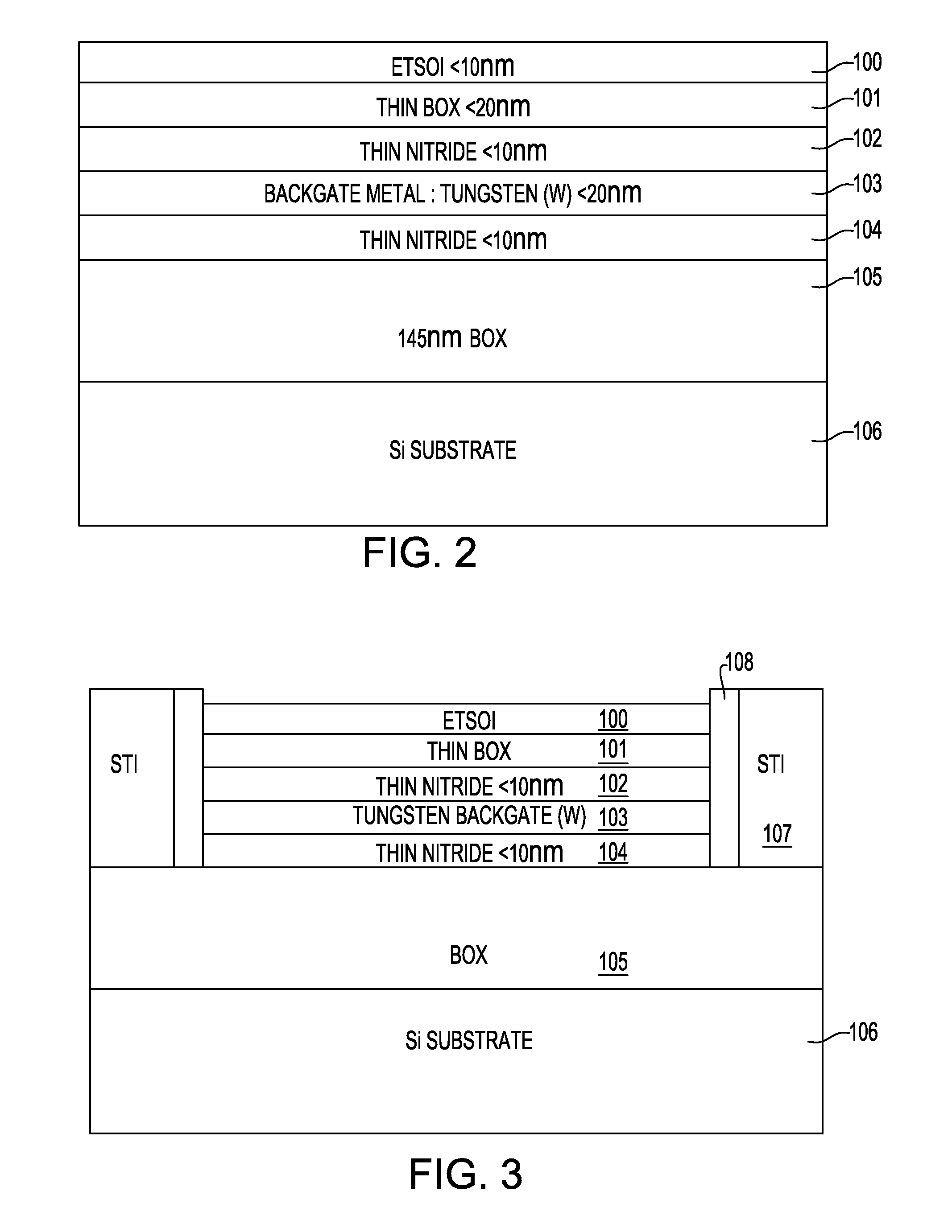
Silicon-on-insulator (SOI) structures with silicon layers less than 20 nm thick are used to form extremely thin silicon-on-insulator (ETSOI) semiconductor devices. ETSOI devices are manufactured using a thin tungsten backgate encapsulated by thin nitride layers to prevent metal oxidation, the tungsten backgate being characterized by its low resistivity. The structure further includes at least one FET having a gate stack formed by a high-K metal gate and a tungsten region superimposed thereon, the footprint of the gate stack utilizing the thin SOI layer as a channel. The SOI structure thus formed controls the Vt variation from the thin SOI thickness and dopants therein. The ETSOI high-K metal backgate fully depleted device in conjunction with the thin BOX provides an excellent short channel control and significantly lowers the drain induced bias and sub-threshold swings. The present structure supports the evidence of the stability of the wafer having a tungsten film during thermal processing, and especially during STI and contact formation.

Description

FIELD OF THE INVENTION[0001]The present invention relates generally to semiconductor devices, and more particularly, to CMOS thin-BOX Backgate Extremely Thin Silicon-On-Insulator (ETSOI) devices to reduce short-channel effects by using metal backgate control.BACKGROUND AND RELATED ART[0002]With shrinking dimensions of various integrated circuit components, transistors such as field-effect transistors (FETs) have experienced dramatic improvement in both performance and power consumption. These improvements may be largely attributed to the reduction in dimensions of components used therein, which in general translate into reduced capacitance, resistance, and increased through-put current from the transistors. Nevertheless, performance improvement brought up by this type of “classic” scaling, in device dimensions, has recently met obstacles and in some cases even been challenged, when the scaling goes beyond a certain point, by the increase in leakage current and variability that are i...

Claims


Application Information

Patent Timeline
Patent Type & Authority Patents(United States)
IPC IPC(8): H01L29/76
CPCH01L21/7624H01L29/66628H01L29/66772H01L29/78603H01L29/78645H01L29/78648H01L29/78696H01L29/7827
Inventor CHAN, KEVIN K.REN, ZHIBINWANG, XINHUI
Owner IBM CORP
Learn More