
Method and calculator for modeling non-equilibrium spin polarized charge transport in nano-structures

a quantum transport and calculator technology, applied in the field of atomistic quantum transport, can solve the problems of inability to demonstrate etching, patterning, etc., and the inability to integrate, and the inability to solve the reliability of spintronics devices

Active Publication Date: 2011-12-20
MCGILL UNIV
View PDF1 Cites 11 Cited by
  • Summary
  • Abstract
  • Description
  • Claims
  • Application Information

AI Technical Summary

Benefits of technology

This approach allows for precise calculations of spin-polarized quantum transport in 3D nanoelectronic devices under non-equilibrium conditions, providing quantitative predictions for TMR devices and aligning with experimental data, including the effect of bias voltage on TMR ratio and current-voltage characteristics.

Problems solved by technology

Spin-based electronics is an emerging disruptive technology with enormous potential.
Indeed, spintronics do not use the same materials used in conventional semiconductors.
Their use in conjunction with traditional semiconductor materials results in challenges in terms of compatibility, integration, etching, patterning, and production.
A second challenging factor is the reliability of spintronics device, which is not demonstrated yet.
A third restraining factor might be the fact that MRAMs requires high current for the magnet to switch between states, which causes problem for low-power operation.
As the devices continue to downsize into the nanoscale limit, currently available modeling methods are no longer adequate or even valid, and new methods are needed to continue to support research and development.
This is especially true due to the fact that there still exist many experimental facts that have not been understood.
It is clear that all the modeling methods presented in literature, while useful for academic research, are not capable of making quantitative predictions of spin-polarized quantum transport for practical TMR devices at the atomistic level under nonequilibrium conditions.
Theoretical modeling of spin-polarized transport including atomic and material properties is a very difficult problem.
However, it still cannot be used for spin polarized charge transport in 3-dimensional magnetic devices.
The existing atomistic modeling methods for TMR devices can be roughly categorized into three classes:(i) Non-self-consistent tight binding methods can account for some qualitative features of transport, but they depend on semi-empirical parameters thereby having limited predictability (H. Mehrez et. al.
ASA is, in fact, an “art” and the results often depend how it is applied (For example, it has been shown that calculated tunneling conductance of Fe—GaAs interface sensitively depends on how ASA is applied, making quantitative predictions very difficult to make. K. Xia, private communication (2005)).
Finally, the method requires very large computational time; and it is unclear if a bias and gate voltage can be modeled.
This method is limited for application in systems consisting of layers of materials.(iii) LMTO method has also been successfully applied to investigate TMR systems at zero bias voltage (K. M. Schep, et al., Phys. Rev. B 56, 10805 (1997); K. Xia, et al.
It is also based on ASA, and has difficulty in applying to non-space filling situations such as molecular TMR structures.
In addition, at present no LMTO methods for TMR device simulation has and can include a bias voltage in the required self-consistent manner.
Present implementations of this method can only be applied to bulk materials or layered bulk materials without external bias or gate voltage.
The above existing methods prove to be limited in their application domain.
In particular, they have only been applied to bulk systems at zero external potential.

Method used


Image

  • Method and calculator for modeling non-equilibrium spin polarized charge transport in nano-structures
  • Method and calculator for modeling non-equilibrium spin polarized charge transport in nano-structures
  • Method and calculator for modeling non-equilibrium spin polarized charge transport in nano-structures

Examples


Embodiment Construction

[0046]The present invention is illustrated in further details by the following non-limiting examples.

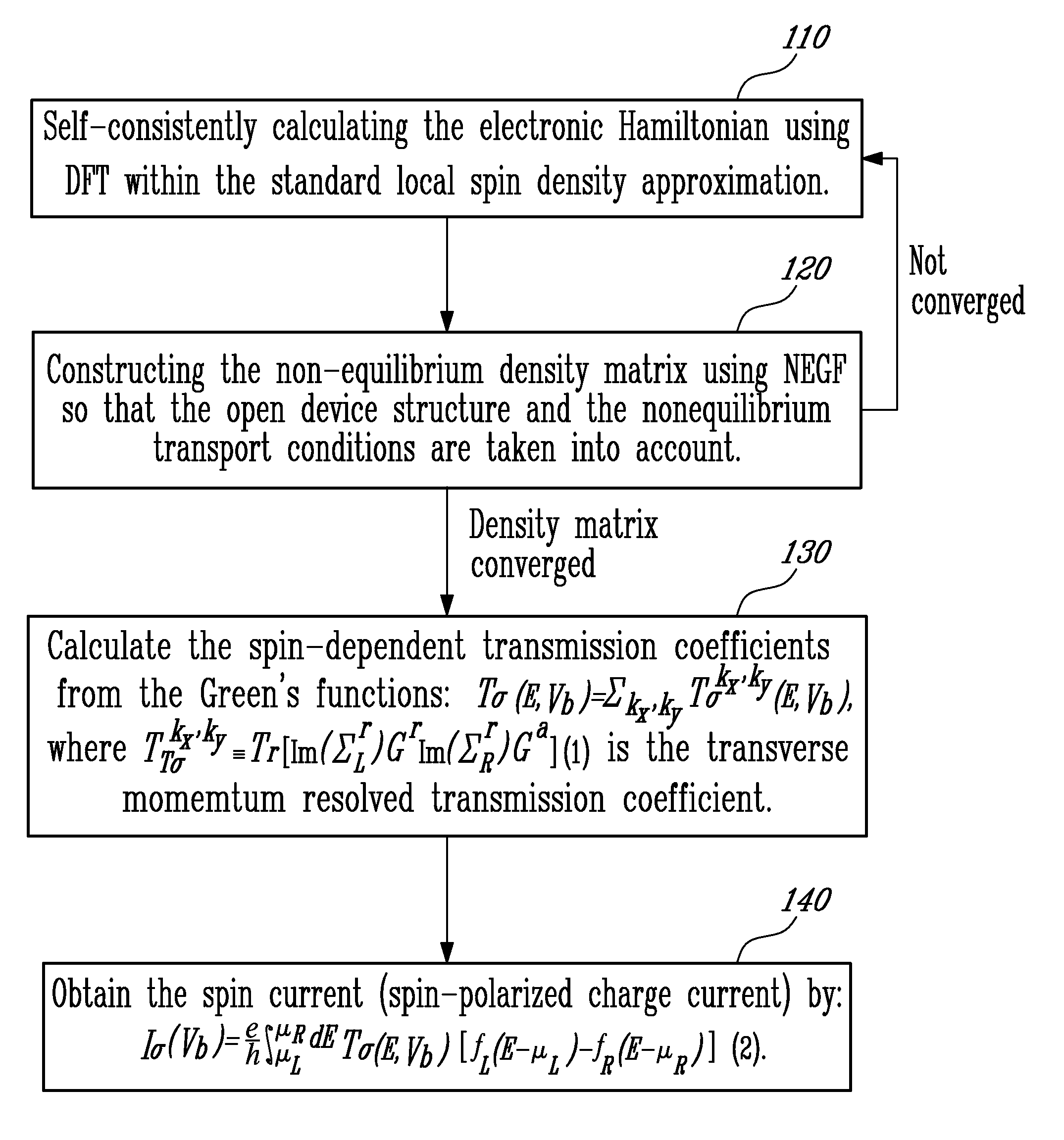
[0047]There is provided a method and a calculator for calculating spin polarized quantum transport in 3-dimensional nanoelectronic devices under finite bias voltage. The method and calculator perform first principles calculations of spin polarized quantum transport in 3-dimensional atomic-scale spintronics (spin electronics) devices under finite bias voltage (externally applied electric field).

[0048]Generally stated, the present method and calculator are based on implementing Density Function Theory (DFT) in combination with Keldysh non-equilibrium Green's functions (NEGF) within the Local Spin Density Approximation (LSDA) and Generalized Gradient Approximation (GGA). The local spin-density approximation (LSDA) is a generalization of the local-density approximation (LDA), in which the functional depends only on the density at the coordinate where the functional is evaluated, to inclu...


PUM


Abstract

A method and calculator for obtaining spin polarized quantum transport in 3-dimensional atom-scale spintronic (spin electronics) devices under finite bias voltage, based on implementing Density Function Theory (DFT) in combination with the Keldysh non-equilibrium Greens function (NEGF) formalism to calculate spin polarized quantum transport in 3-dimensional nanostructures under finite bias and external voltage.

Description

CROSS REFERENCE TO RELATED APPLICATIONS[0001]This application claims priority on U.S. provisional application No. 60 / 885,056, filed on Jan. 16, 2007. All documents above are herein incorporated by reference.FIELD OF THE INVENTION[0002]The present invention relates to atomistic quantum transport. More specifically, the present invention is concerned with a method and a calculator for calculating spin polarized quantum transport in 3-dimensional nanoelectronic devices under finite bias voltage. All documents below are herein incorporated by reference.BACKGROUND OF THE INVENTION[0003]Spin-based electronics is an emerging disruptive technology with enormous potential. A promising application is the field of computer memories, where Magnetoresistive Random Access Memories (MRAM) could replace the present memory technologies.[0004]The rapid progress in the miniaturization of semiconductor electronic devices leads to a degree of integration where quantum effects will take precedence over c...

Claims


Application Information

Patent Timeline
Patent Type & Authority Patents(United States)
IPC IPC(8): G06F17/10G06N99/00
CPCB82Y10/00G11C11/16H01L29/66984H01L43/08H10N50/10
Inventor GUO, HONGWALDRON, DEREKLARADE, BRIAN
Owner MCGILL UNIV
Learn More