Eureka AIR delivers breakthrough ideas for toughest innovation challenges, trusted by R&D personnel around the world.

Multi-pitch scatterometry targets

a scatterometry and target technology, applied in the field of substrate processing, can solve the problems of conventional metrology targets and techniques that do not provide the necessary parameter sensitivity required

Active Publication Date: 2011-09-20
TOKYO ELECTRON LTD
View PDF26 Cites 16 Cited by
  • Summary
  • Abstract
  • Description
  • Claims
  • Application Information

AI Technical Summary

Problems solved by technology

Conventional metrology targets and techniques do not provide the necessary parameter sensitivity required to detect and differentiate the variation due to focus, dose, and PEB temperature

Method used


Image

  • Multi-pitch scatterometry targets
  • Multi-pitch scatterometry targets
  • Multi-pitch scatterometry targets

Examples


Embodiment Construction

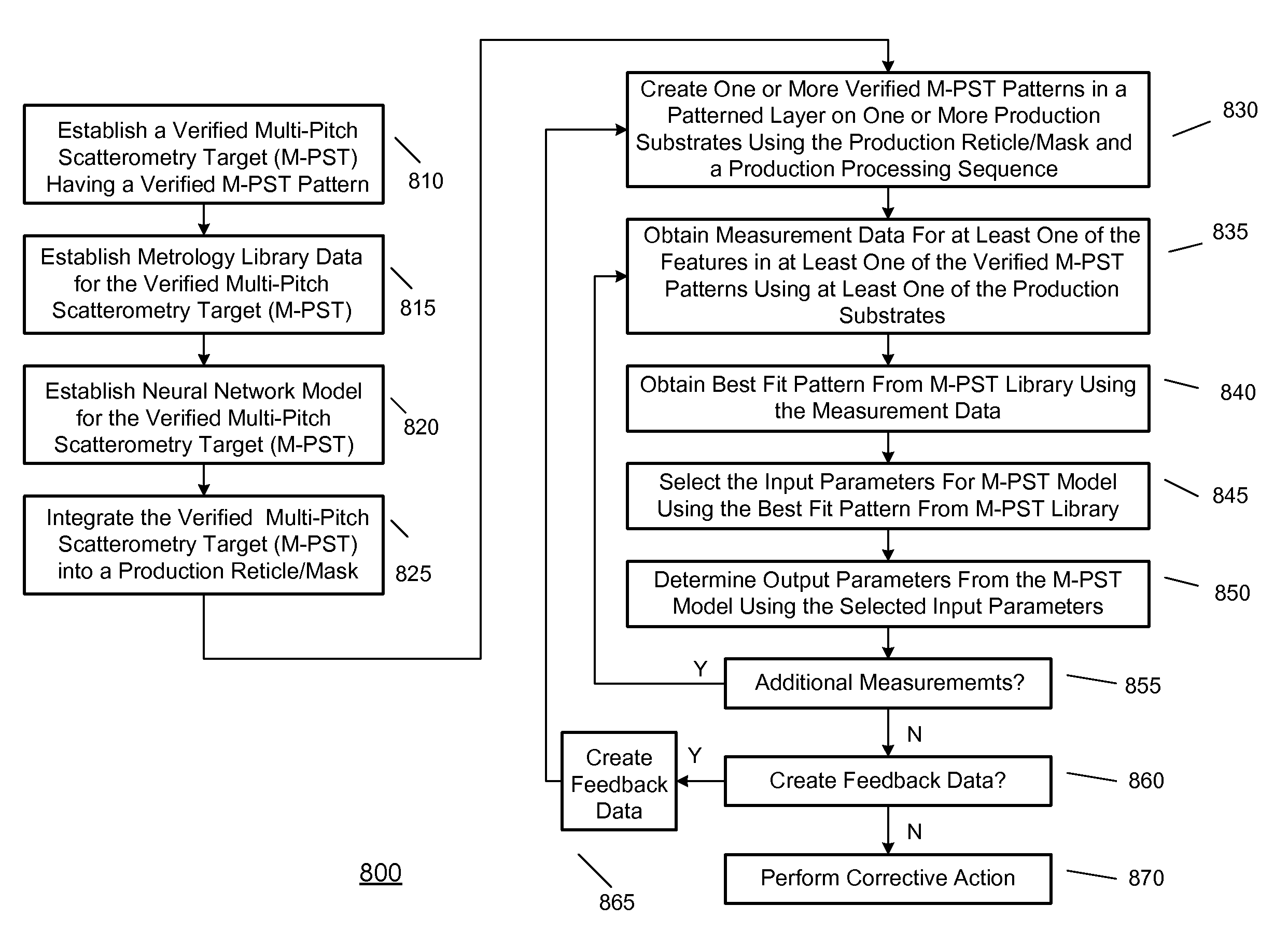
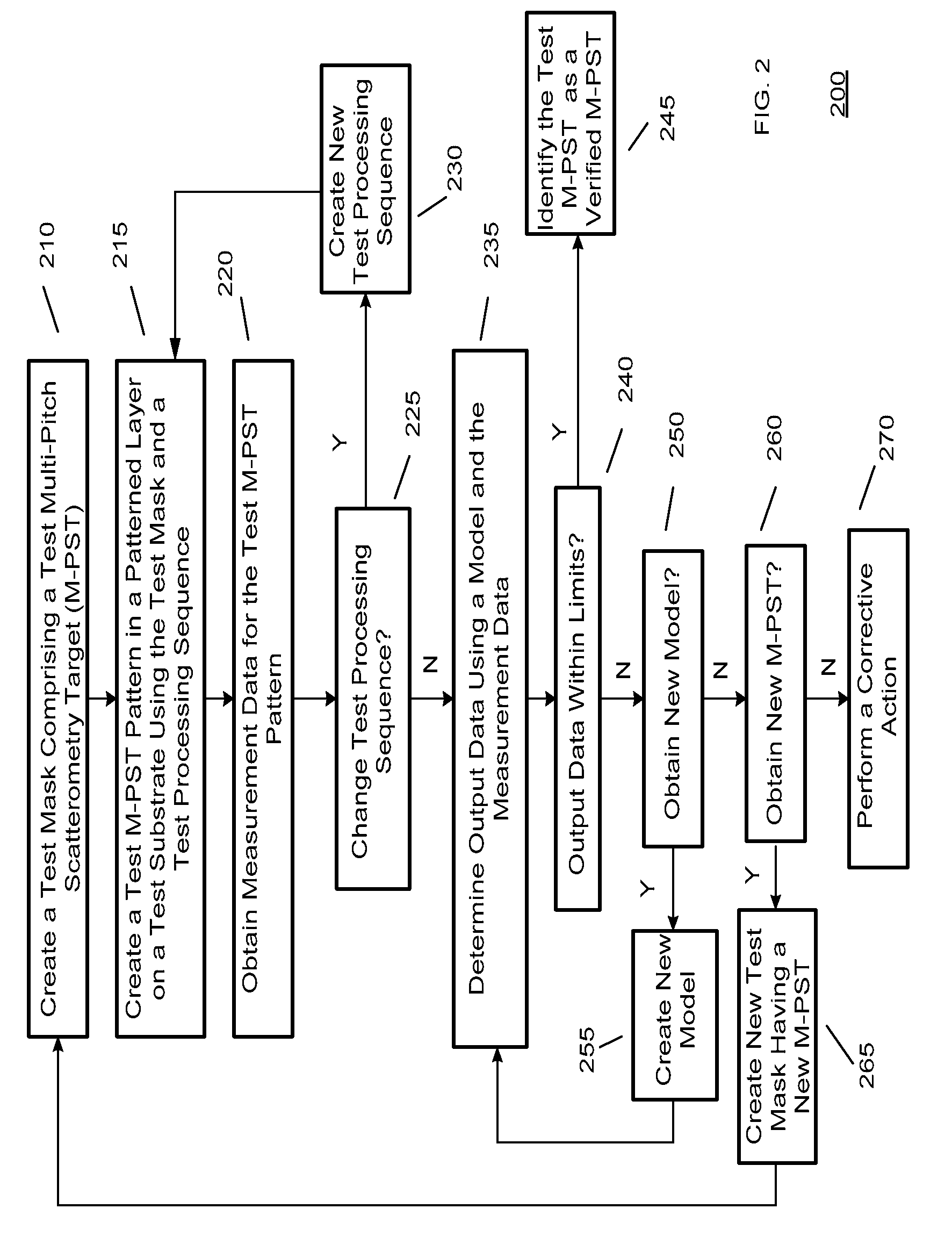
[0021]The invention can provide apparatus and methods of processing a substrate using multi-pitch scatterometry targets (M-PSTs) that have critical dimension (CD) and sidewall angle (SWA) sensitivity to exposure focus variations, exposure dose variations, and post exposure bake (PEB) temperature variations. In addition, the CD and SWA data can be de-convolved so that the individual measurement process variable contributors can be identified. The M-PSTs can be used in Double-Patterning (D-P) processing sequences, Double-Exposure (D-E) processing sequences, or Single-Patterning (S-P) processing sequences, or any combination thereof to control transistor structures. The S-P, D-P, and / or D-E processing sequences can include one or more lithography-related procedures, one or more scanner-related procedures, one or more etch-related procedures, one or more deposition-related procedures, one or more measurement-related procedures, or one or more inspection-related procedures, or any combin...


PUM

PropertyMeasurementUnit
thicknessaaaaaaaaaa
sizesaaaaaaaaaa
wavelengthaaaaaaaaaa

Abstract

The invention can provide a method of processing a substrate using multi-pitch scatterometry targets (M-PSTs) for de-convolving lithographic process parameters during Single-Patterning (S-P), Double-Patterning (D-P) procedures, and Double-Exposure (D-E) procedures used to control transistor structures. The M-PSTs) can have critical dimension (CD) and sidewall angle (SWA) sensitivity to exposure focus variations, exposure dose variations, and post exposure bake (PEB) temperature variations. In addition, the variation can be de-convolved so that the individual measurement process variable contributor can be identified.

Description

BACKGROUND OF THE INVENTION[0001]1. Field of the Invention[0002]The present invention relates to substrate processing, and more particularly to improving the substrate processing by using multi-pitch scatterometry targets for de-convolving lithographic process parameters during Single-Patterning (S-P) procedures, Double-Patterning (D-P) procedures, and Double-Exposure (D-E) procedures.[0003]2. Description of the Related Art[0004]Many multiple patterning techniques are currently being used during semiconductor substrate processing to increase the number of features and / or structures within devices on a substrate. Multiple patterning techniques can include double exposure techniques, double patterning techniques, spacer techniques, mask techniques, and brute force techniques. In 2006, the International Technology Roadmap for Semiconductors was expanded to include double patterning as a potential solution for 32 nm (nanometer) lithography. Multiple patterning techniques are viewed by s...

Claims


Application Information

Patent Timeline
Patent Type & Authority Patents(United States)
IPC IPC(8): G06F17/50G06F19/00G21K5/00G03F1/00H01L21/00
CPCG03F1/14G03F7/70625G03F7/70641G03F1/44
Inventor CARCASI, MICHAEL A.DIXON, DAVID
Owner TOKYO ELECTRON LTD
Why Eureka
Eureka Blog
Learn More