Process for forming dielectric films

a dielectric film and film technology, applied in the field of forming dielectric films, can solve the problems of reducing the capacitance increasing power consumption disadvantageously, and reducing the length of gate dielectric films, so as to achieve high permittivity, high productivity, and precise controllability.

Active Publication Date: 2011-09-06
CANON KK +1
View PDF11 Cites 1 Cited by
  • Summary
  • Abstract
  • Description
  • Claims
  • Application Information

AI Technical Summary

Benefits of technology

[0015]To solve the above technical problems, the present invention intend to produce high permittivity dielectric films with a precise controllability and at a high productivity.
[0039]According to the present invention, high permittivity dielectric films suitable for use as a high permittivity gate dielectric films can be formed with precise controllability and high productivity.

Problems solved by technology

However, the shortening of the channel length lowers the capacitance of the gate dielectric films and retards the switching operation of the transistors.
However, the decrease of the thickness of the gate dielectric films to several nanometers tends to cause a larger amount of gate leakage current to increase the power consumption disadvantageously.
However, the film formed by MOCVD contains a large amount of residual impurities like carbon and hydrogen coming from the starting organic material.
The residual impurities tend to cause a large quantity of a leakage current in the formed film.
A longer time of oxidation by this method to diffuse the metal atoms enough into the silicon dioxide film can cause excessive oxidation.
On the other hand, in the method of Japanese Patent Application Laid-Open No. 2002-314074, in which thermal oxidation is conducted at a high temperature to diffuse the metal atoms in a short time, the underlying silicon substrate tends to be oxidized to increase excessively the thickness of the silicon dioxide film.
In the method of Japanese Patent Application Laid-Open No. 2003-297814, in which the metal atoms are diffused only by irradiation of energetic particles, the thickness of the remaining silicon dioxide film cannot readily be controlled.
As described above, in conventional techniques, the diffusion of the metal into the silicon dioxide film and the mixing of the silicon dioxide film with the metal film cannot readily be controlled, and the conditions of diffusion of the metal atoms and the conditions of the oxidation of metal film cannot be controlled independently.
Thus conventional techniques cannot produce dielectric films having a desired film thickness with a high productivity.

Method used


Image

  • Process for forming dielectric films
  • Process for forming dielectric films
  • Process for forming dielectric films

Examples


example 1-1

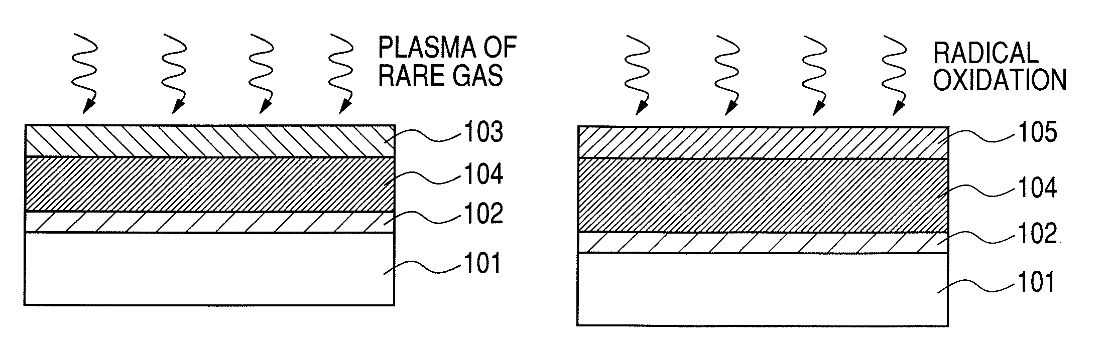
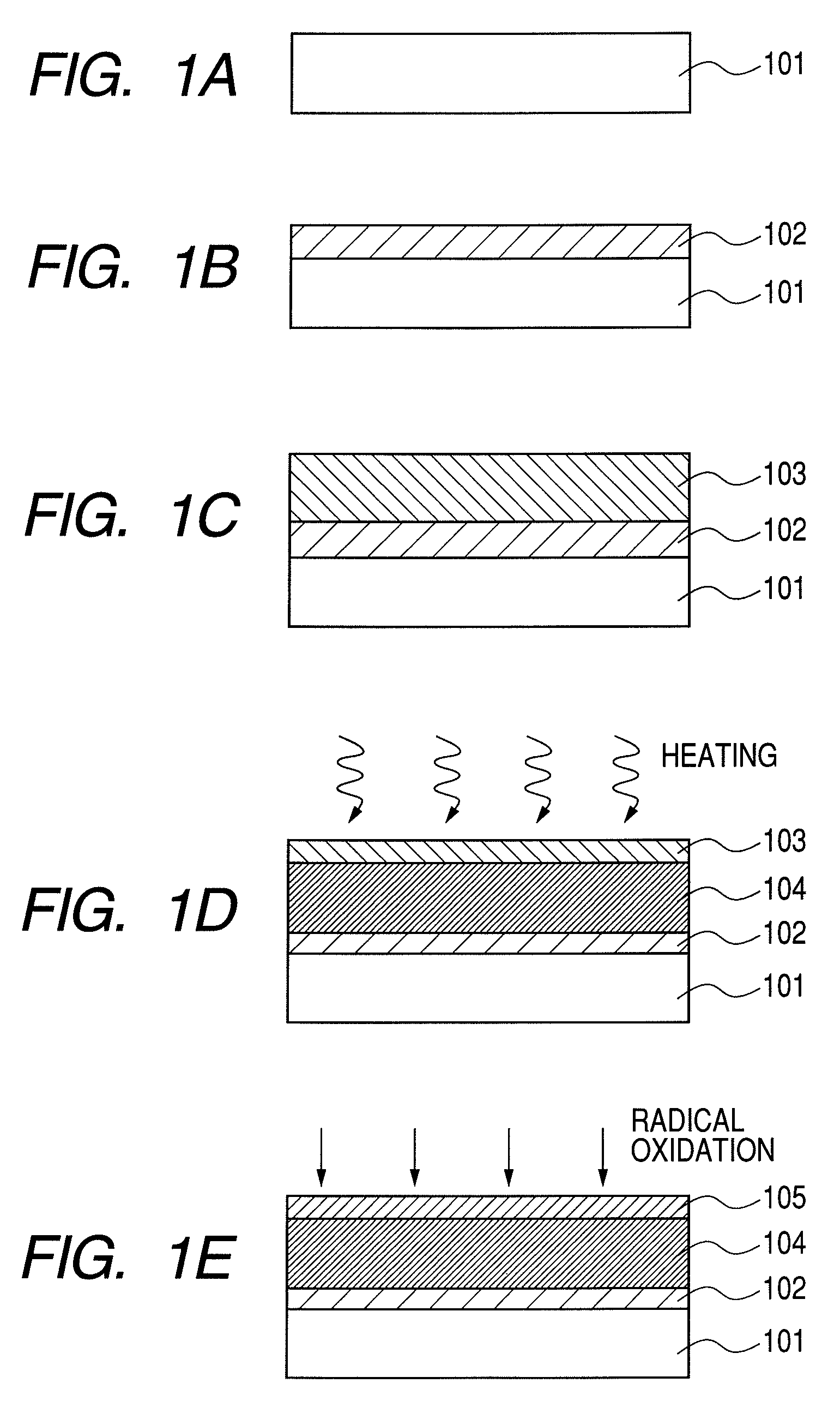
[0073]The process of this Example was conducted as illustrated in FIGS. 1A to 1E. Silicon substrate 101 was a p-type monocrystalline silicon substrate of 200 mm diameter.

[0074]Firstly, the surface of substrate 101 was cleaned by RCA cleaning to eliminate impurities and a native oxide film.

[0075]Next, substrate 101 was transferred to a high-speed thermal oxidation equipment and was thermally oxidized in an oxygen atmosphere at 1000° C. to form silicon dioxide film 102 of 2 nm thick on the surface layer of substrate 101.

[0076]Subsequently, substrate 101 having silicon dioxide film 102 was transferred into an RF magnetron type sputtering equipment not shown in the drawing. The target of the sputtering equipment was constituted of Hf. The sputtering equipment holding the substrate inside was evacuated to a vacuum of 2.6×10⁻³ Pa. Substrate 101 was heated by a heating means and was kept at 300° C. Thus oxygen and moisture which can oxidize the metal film in the deposition of the metal fil...

example 1-2

[0082]The process of this Example was conducted as illustrated in FIGS. 1A to 1E. Silicon substrate 101 used was a p-type monocrystalline silicon substrate of 200 mm diameter.

[0083]The substrate was treated through the steps to the radical oxidation in the same manner as in Example 1-1.

[0084]In the next step of nitridation, substrate 101 having films 102, 104, 105 was transferred into a plasma equipment which generates nitrogen radicals by surface-wave plasma.

[0085]The plasma equipment was evacuated, and N2 gas was introduced into the plasma equipment at a flow rate of 200 sccm. The pressure inside the plasma equipment was kept at 26 Pa. In this step, the temperature of substrate 101 was kept at 200° C. by heater incorporated in a substrate-supporting stage for heating the substrate. A microwave of 2.45 GHz was emitted from an antenna and was introduced into the plasma equipment through a dielectric wall for keeping the vacuum in the equipment to generate surface-wave plasma. With t...

example 1-3

[0088]The process of this Example was conducted according to the embodiment illustrated in FIGS. 1A to 1E. Silicon substrate used was a P-type monocrystalline silicon substrate of 200 mm diameter.

[0089]In this Example, silicon dioxide film 102 in the surface layer of substrate 101 had a thickness of 1.6 nm, and metal film 103 was formed by sputtering in a thickness of 1 nm. After the formation of the films, the substrate having the films was treated through the steps to the radical oxidation to prepare a sample in the same manner as in Example 1-1 except that the temperature and time of the heat treatment after formation of the metal film were changed as shown in Table 1 below.

[0090]

TABLE 1HeatingConditionstemperatureHeating time1600° C.60 seconds2700° C.60 seconds3600° C.120 seconds 

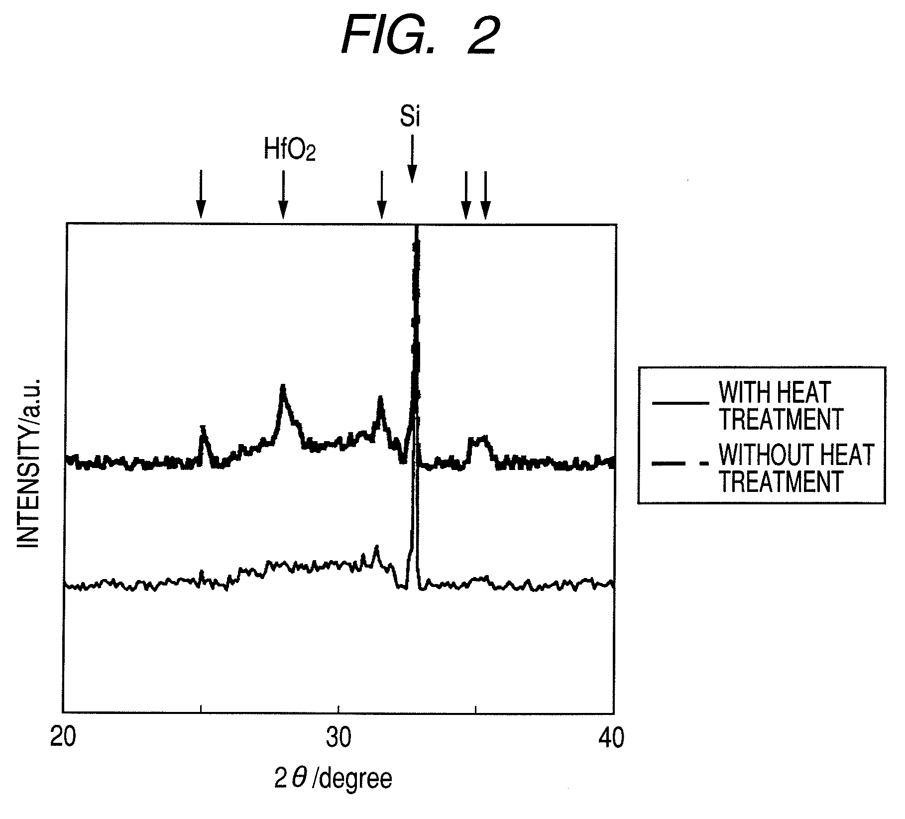
[0091]The distributions of the elements in the film thickness direction (depth direction) in the insulating film of the test sample piece were measured by RBS. FIGS. 3A to 3C show the measured distribut...


PUM

PropertyMeasurementUnit
thicknessaaaaaaaaaa
partial pressureaaaaaaaaaa
temperatureaaaaaaaaaa

Abstract

A process for forming dielectric films containing at least metal atoms, silicon atoms, and oxygen atoms on a silicon substrate comprises a first step of oxidizing a surface portion of the silicon substrate to form a silicon dioxide film; a second step of forming a metal film on the silicon dioxide film in a non-oxidizing atmosphere; a third step of heating in a non-oxidizing atmosphere to diffuse the metal atoms constituting the metal film into the silicon dioxide film; and a fourth step of oxidizing the silicon dioxide film containing the diffused metal atoms to form the film containing the metal atoms, silicon atoms, and oxygen atoms.

Description

BACKGROUND OF THE INVENTION[0001]1. Field of the Invention[0002]The present invention relates to a process for forming dielectric films, particularly to a process for forming dielectric films suitable for use as high permittivity gate dielectric films in a semiconductor device.[0003]2. Description of the Related Art[0004]In semiconductor devices like MOS (metal oxide semiconductor) type transistors, channel lengths are made shorter and shorter to increase the operation speed. However, the shortening of the channel length lowers the capacitance of the gate dielectric films and retards the switching operation of the transistors. Therefore to obtain a sufficient capacitance for the switching operation of the transistors, the gate dielectric films are made thinner. Conventionally as the material for the dielectric films of MOS type transistors, silicon dioxide (SiO2) is used owing to ease of the production and the resulting satisfactory interfacial properties of the film. However, the d...

Claims


Application Information

Patent Timeline
Patent Type & Authority Patents(United States)
IPC IPC(8): H01L29/72
CPCC23C14/185C23C14/34C23C14/5853C23C14/5893H01L21/02074H01L21/28185H01L21/28229H01L21/3105H01L21/3145H01L21/31645H01L21/321H01L29/513H01L29/517H01L21/02238H01L21/02142H01L21/31H01L21/02356H01L21/0234H01L21/02332
Inventor KITANO, NAOMUFUKUCHI, YUSUKESUZUKI, NOBUMASAKITAGAWA, HIDEO
Owner CANON KK
Why Eureka
Try Eureka