Increased grain size in metal wiring structures through flash tube irradiation
a technology of metal wiring and flash tube, which is applied in the direction of basic electric elements, electrical equipment, semiconductor devices, etc., can solve the problems of increasing the length of the wire, increasing the size of the crystalline grains, and increasing the surface irregularities, so as to achieve small surface irregularities and low specific resistance
- Summary
- Abstract
- Description
- Claims
- Application Information
AI Technical Summary
Benefits of technology
Problems solved by technology
Method used
Image

Examples
first embodiment
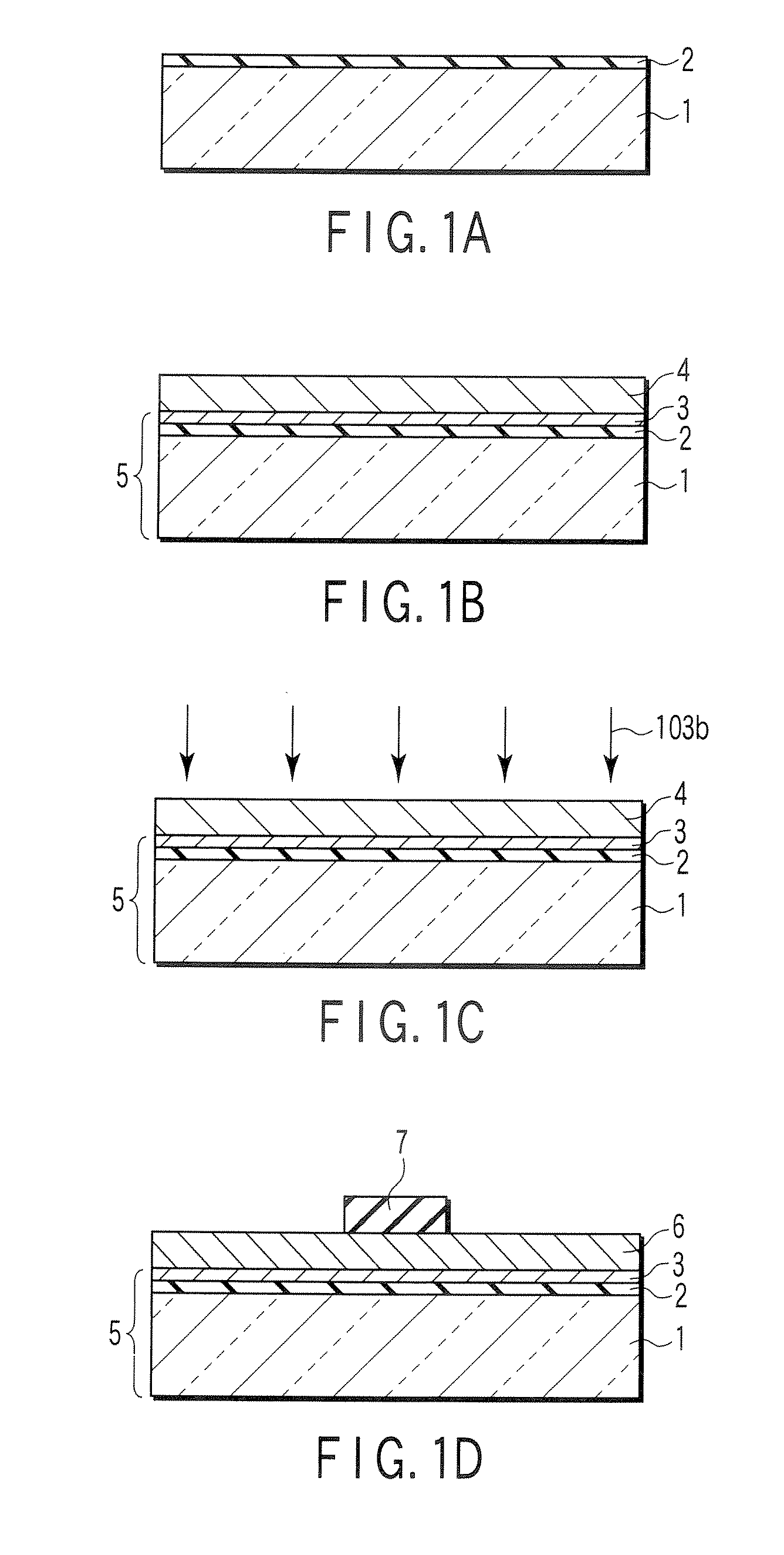
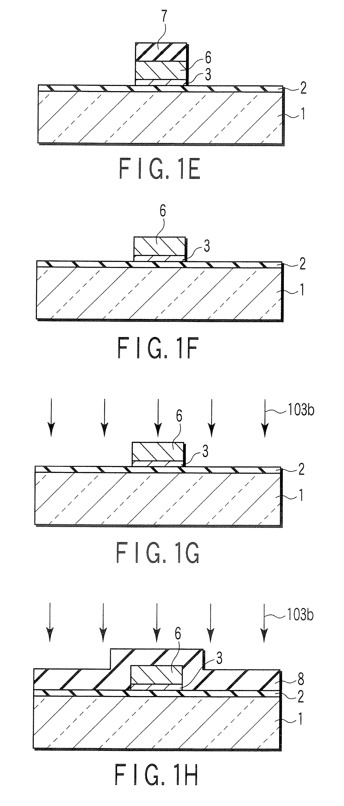
[0039]Hereinafter, the present invention will be described with reference to FIGS. 1A to 2. In the present embodiment, one aspect of a wiring structure according to the invention will be described here. FIGS. 1A to 1H show a process for manufacturing a wiring structure according to the present embodiment.
[0040]First, as shown in FIG. 1A, a metal or insulator substrate, for example, a rectangular substrate 1 made of a glass is prepared. An undercoat insulating layer 2 made of silicon nitride (SiNx), silicon oxide (SiO2) or the like, having a predetermined thickness, for example, a film thickness of 300 nm, is formed at a whole portion or a selected portion on the surface or the top face of the substrate 1.
[0041]Next, as shown in FIG. 1B, a barrier metal layer 3 having a predetermined thickness, for example, a film thickness of 30 nm is formed on the undercoat insulating layer 2. The barrier metal layer 3 is intended to restrict substances contained in a metal layer 4 described later ...
second embodiment
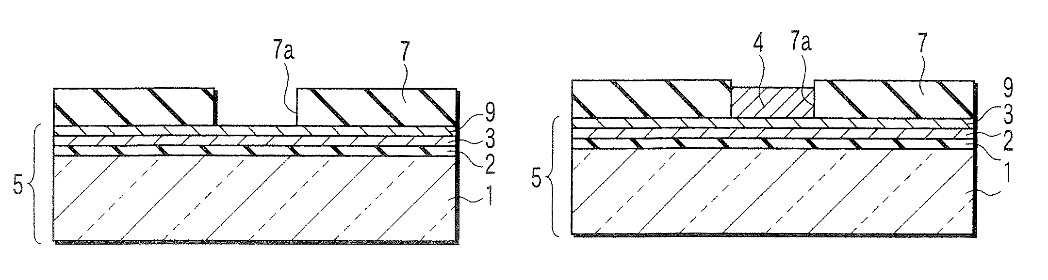
[0065]Hereinafter, the present invention will be described with reference to FIGS. 9A to 9G. The present embodiment describes another aspect of the wiring structure according to the present invention.
[0066]The process shown in FIG. 9A is identical to that shown in FIG. 1A according to the first embodiment described above. Next, as shown in FIG. 9B, a barrier metal layer 3 and a seed layer 9 (for example, a copper seed layer made of copper or consisting essentially of copper) are sequentially continuously formed on an undercoat insulating layer 2. In this case, the undercoat insulating layer 2, the barrier metal layer 3, and the seed layer 9 formed on the substrate 1 serve as a base substance 5. The seed layer 9 forms a wiring structure 6 later together with the metal layer 4.
[0067]Next, a photoresist film 7 is formed on the seed layer 9, and, as shown in FIG. 9C, a resist groove 7a is formed on the photoresist film 7 such that the surface of the seed layer 9 is exposed on only a des...
third embodiment
[0079]Now, with reference to FIGS. 11 to 13, a description will be given with respect to a method for forming a wiring structure and a semiconductor according to the present invention. While the present embodiment describes a method for manufacturing a bottom gate type amorphous silicon TFT as a method for manufacturing a semiconductor device, the semiconductor device is not limited thereto.
[0080]FIG. 11 schematically depicts an example of an equivalent circuit of an active matrix type liquid crystal display device 10 that serves as a display device. The liquid crystal display device 10 comprises: a pair of transparent substrates 11 and 12; a liquid crystal layer 13; an undercoat insulating layer 14; a pixel electrode 15; a scanning line 16 formed of a wiring structure 6; a signal line 17; an opposite electrode 18; a thin-film transistor 19 (hereinafter, referred to as a TFT) serving as a semiconductor device or a driving element; a scanning line drive circuit 21; a signal line driv...
PUM
| Property | Measurement | Unit |
|---|---|---|
| thickness | aaaaa | aaaaa |
| thickness | aaaaa | aaaaa |
| thickness | aaaaa | aaaaa |
Abstract
Description
Claims
Application Information
 - R&D
- Intellectual Property
- Life Sciences
- Materials
- Tech Scout
- Unparalleled Data Quality
- Higher Quality Content
- 60% Fewer Hallucinations
Browse by: Latest US Patents, China's latest patents, Technical Efficacy Thesaurus, Application Domain, Technology Topic, Popular Technical Reports.
© 2025 PatSnap. All rights reserved.Legal|Privacy policy|Modern Slavery Act Transparency Statement|Sitemap|About US| Contact US: help@patsnap.com