Method of producing through wiring substrate and method of producing device

a technology of wiring substrate and wiring layer, which is applied in the direction of mechanical vibration separation, semiconductor/solid-state device details, instruments, etc., can solve the problems of high resistivity of through wiring, deformation, permanent deformation, damage, etc., to increase reduce temperature, and improve the degree of integration of elements

Active Publication Date: 2018-03-27
CANON KK
View PDF3 Cites 3 Cited by
  • Summary
  • Abstract
  • Description
  • Claims
  • Application Information

AI Technical Summary

Benefits of technology

[0012]With the production methods according to the present disclosure, the degree of the surface irregularities of the inner wall of the through hole is larger, and the surface of the through wiring is more strongly restrained on the first surface side of the substrate. In contrast, the degree of the surface irregularities of the inner wall of the through hole is smaller, and the surface of the through wiring more freely moves on the second surface side of the substrate. Furthermore, with the structure of the device according to the present disclosure, in the step of producing the element structure, permanent deformation of or damage to the thin film or the like near the through wiring due to an increase and a decrease in temperature can be reduced. Accordingly, the element can be disposed in the proximity of the through wiring. This can increase the degree of integration of elements. Furthermore, quality of the thin film formed on the inner wall of the through hole and the upper side of the through hole is high. This can make the device more electrically reliable.

Problems solved by technology

However, the through wirings formed of polysilicon have a drawback of having a high resistivity.
This may cause a thin film included in each element to be, for example, deformed, permanently deformed, or to be damaged.
Furthermore, when the temperature decreases, such a wiring attempts to return to its original state and draws the thin film.
This may cause, in the proximity of the end surface, the thin film to be permanently deformed, damaged, or stress in the thin film may increase.
Such permanent deformation of the thin film, damage to the thin film, an increase in stress in the thin film, and so force may cause deficiency of the element and variation of the performance among the elements.
In this case, however, the degree of integration of elements reduces.
Due to this stress, the scallops and the thin film formed on the scallops may be eternally deformed or damaged, and accordingly, desired functions are not necessarily performed.

Method used


Image

  • Method of producing through wiring substrate and method of producing device
  • Method of producing through wiring substrate and method of producing device
  • Method of producing through wiring substrate and method of producing device

Examples


first embodiment

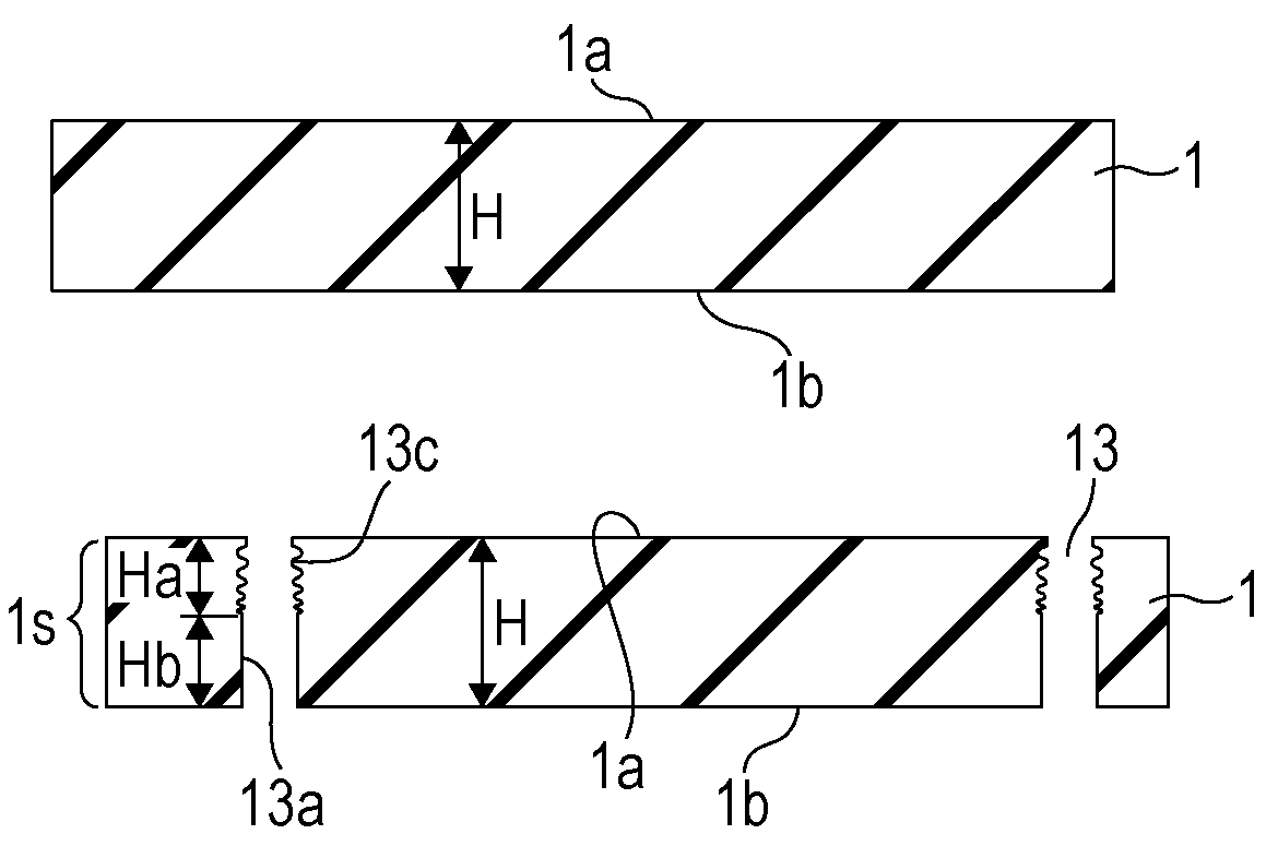
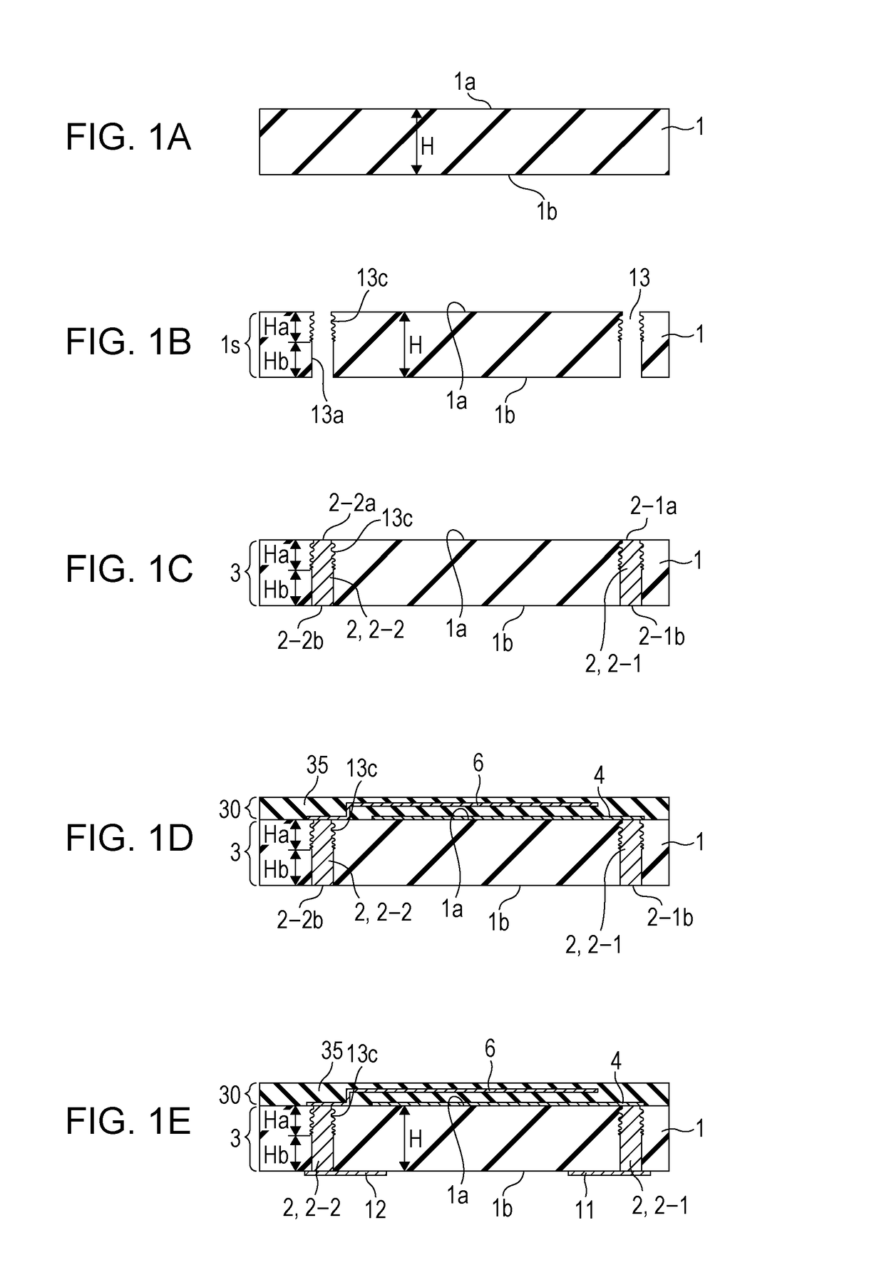
[0026]A first embodiment of a method of producing a device according to one or more aspects of the present disclosure is described with reference to FIGS. 1A to 1E. FIGS. 1A to 1E are sectional views illustrating the present embodiment. Although a plurality of through wirings or a plurality of elements are simultaneously formed in a single substrate in typical production of the device, only two through wirings and a single element are illustrated in FIGS. 1A to 1E as appropriate for ease of seeing by simplifying illustration.

[0027]Initially, as illustrated in FIG. 1A, a first substrate 1 is prepared. The first substrate 1 is formed of an insulating material such as glass or a semiconductor material such as Si. The first substrate 1 includes a first surface 1a and a second surface 1b positioned on the opposite side to the first surface. Both the first surface 1a and the second surface 1b of the first substrate 1 are flat and mirror polished. The thickness of the first substrate 1 is,...

second embodiment

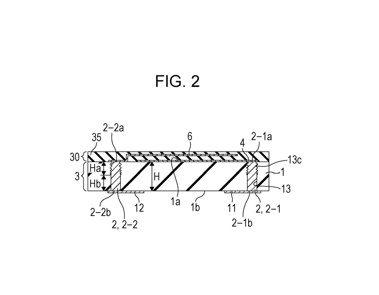
[0042]An embodiment of a structure of the device according to one or more aspects of the present disclosure is described with reference to FIG. 2. FIG. 2 is a sectional view illustrating a second embodiment. Typically, a plurality of through wirings or a plurality of elements are formed in a single device. However, only two through wirings and a single element are illustrated in FIG. 2 for ease of seeing by simplifying illustration.

[0043]As illustrated in FIG. 2, the device according to the present embodiment includes the through wiring substrate 3, the element structure 30, and the electrode pads 11 and 12. The through wiring substrate 3 includes the first substrate 1, the through holes 13 that extend from the first surface 1a to the second surface 1b of the first substrate 1, the second surface 1b being the opposite surface to the first surface 1a, and the through wirings 2 (including the through wirings 2-1 and 2-2) formed of the electrically conductive material with which the in...

first example

[0051]A first example of the method of producing the device according to one or more aspects of the present disclosure is described with reference to sectional views of FIGS. 3A to 3F. For ease of seeing, only two through wirings and a single element are illustrated as appropriate also in FIGS. 3A to 3F.

[0052]Initially, as illustrated in FIG. 3A, the first substrate 1 is prepared. As the first substrate 1, an Si substrate is used. The first substrate 1 includes the first surface 1a and the second surface 1b. These two surfaces are mirror polished so as to have a surface roughness of Ra≤2 nm. The resistivity of the first substrate 1 is about 0.01 Ω·cm. The thickness H of the first substrate 1 is about 300 μm.

[0053]Next, as illustrated in FIG. 3B, the through holes 13 are formed so as to extend from the first surface 1a to the second surface 1b of the first substrate 1. The through holes 13 each have a substantially cylindrical shape. The diameter of the openings in the first surface ...


PUM

PropertyMeasurementUnit
surface roughnessaaaaaaaaaa
heightaaaaaaaaaa

Abstract

In a method of producing a device in which an element structure is provided on a substrate including a through wiring, a through hole is formed so as to extend from a first surface of the substrate to a second surface of the substrate disposed on an opposite side of the substrate to the first surface, the through wiring is formed by filling the through hole with an electrically conductive material, and the element structure is formed on a first surface side. In the step of forming the through hole, a degree of surface irregularities of an inner wall of the through hole is larger on the first surface side than on a second surface side.

Description

BACKGROUND[0001]Field of the Disclosure[0002]The present disclosure relates to a through wiring substrate, a device that includes the through wiring substrate, a method of producing the through wiring substrate, a method of producing the device, and so forth.[0003]Description of the Related Art[0004]For reduction of the sizes of devices and advancement of the functions of the devices such as an increase in speed and an increase in the number of functions, through wirings are used. The through wirings allow chips included in such a device to be electrically connected to one another or elements on the top surface of a substrate to be electrically connected to wiring on the bottom surface of the substrate with smallest distances. The through wirings may be formed by a via-first method or a via-last method. With the via-first method, the through wirings are formed before the elements are formed. With the via-last method, the through wirings are formed after the elements have been formed...

Claims


Application Information

Patent Timeline
Patent Type & Authority Patents(United States)
IPC IPC(8): G01N21/00H05K1/11G01H9/00B06B1/06B06B1/02G01N21/17H05K1/09H05K3/40H05K3/00G01N29/24H05K3/06H05K3/42
CPCG01N21/1702B06B1/06B06B1/0622G01H9/004G01N29/24G01N29/2406G01N29/2418G01N29/2437H05K1/09H05K1/115H05K3/0041H05K3/4084B06B1/0292H05K2203/025G01N2021/1706H05K3/06H05K3/42H05K2201/09854H01L21/76898H01L23/49827H01L21/486
Inventor WANG, SHINANSETOMOTO, YUTAKA
Owner CANON KK
Why Eureka
Try Eureka