
Electrical connector structure of circuit board and method for fabricating the same

a technology of electrical connection and circuit board, which is applied in the direction of resistive material coating, solid-state device application, non-metallic protective coating, etc., can solve the problems of reducing the total area, increasing the quantity of electrical connection pads on the carried components, and unable to meet the development requirements of chips, so as to reduce the requirement of exposure accuracy

Active Publication Date: 2009-10-27
PHOENIX PRECISION TECH CORP
View PDF4 Cites 7 Cited by
  • Summary
  • Abstract
  • Description
  • Claims
  • Application Information

AI Technical Summary

Benefits of technology

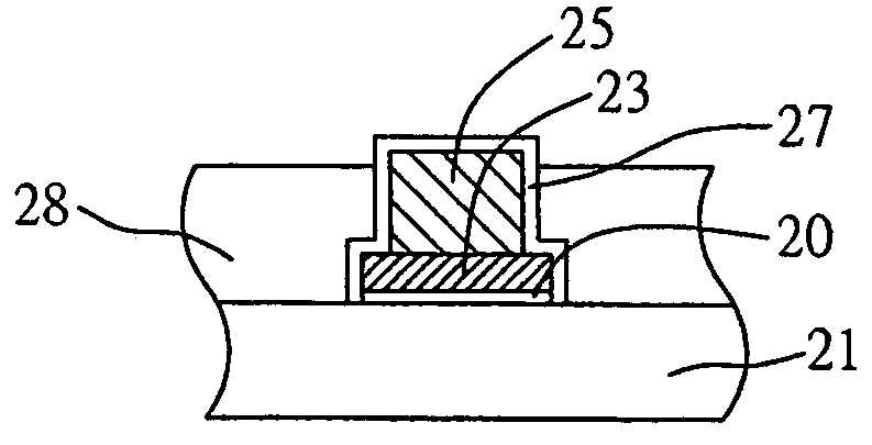
[0012]In light of the above prior-art drawbacks, a primary objective of the present invention is to provide an electrical connection structure of a semiconductor chip and a method of fabricating the same, so as to avoid restrictions on the size of conductive bumps and the pitches formed therebetween, and difficulties of alignment when performing the conventional electroplating process, and reduce requirement of exposure accuracy.

Problems solved by technology

But the change also shrinks the total area of carried components in a chip, which in turn increases the quantity of electrical connection pads on the carried components; as a result, the demands for the development of chip can only be satisfied by shrinking the size and the pitch of electrical connection pads.
But the shrinking of electrical connection pads also makes the openings on the stencil used in stencil printing technology smaller as well.
As a result, the smaller openings on stencil not only increases the cost for producing the stencil, which is resulted from difficulty in stencil production; but also hampers the later production process because the smaller opening on the stencil can be impervious to the soldering material.
Furthermore, apart from the requirement of accurate size of stencil in order to ensure the precision in the shaping of soldering material; there are the problems of the number of times the stencil has been used and cleaned.
Since the soldering material is viscous, it can stick to the inner wall of openings in the stencil and accumulate as the stencil is used to print many times, and this can give rise to incorrect quantity and shape of soldering material from the design specification when the stencil is used next time.
Therefore, when the stencil is put to actual usage, it must be cleaned after a certain times of printing, otherwise problems like conflicting shape and size of soldering material can arise and result in the production process being impeded, which lowers its reliability.
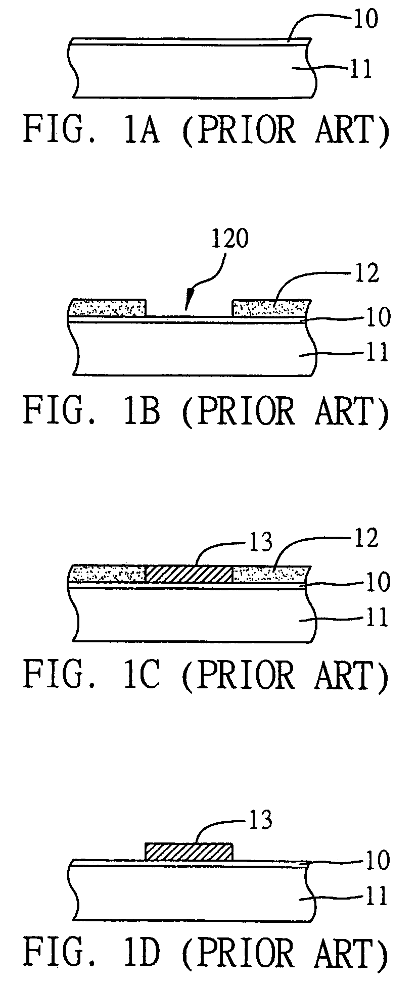
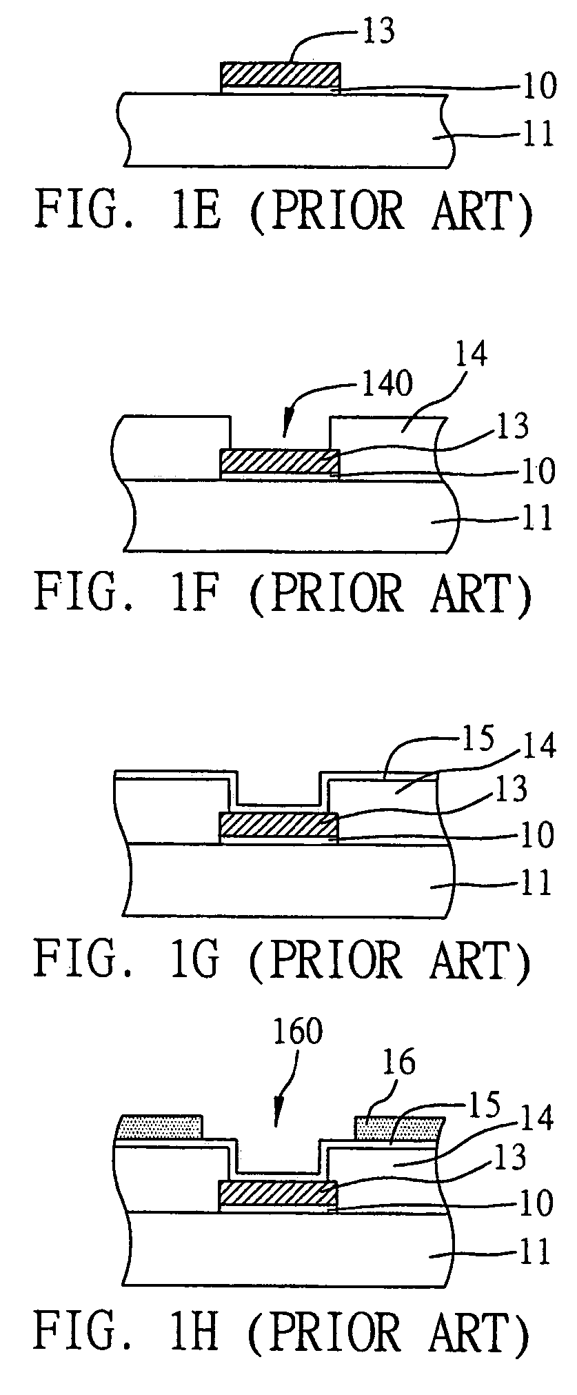
As the range of alignment accuracy of a general machine is approximately 20 μm-30 μm, it is difficult to align the openings of the electroplated resist layer with the center of the opening of the solder mask layer.
Nevertheless, the requirement of forming fine pitches between the electrical connection pads cannot be met if the openings of the electroplated resist layer are enlarged.
Therefore, the conductive bumps cannot be formed on the electrical connection pads having fine pitches therebetween by the electroplating process.
Moreover, if the conductive bumps are to be formed with fine pitches therebetween, the insulating layer and resist layer have to be aligned more accurately, resulting to a increase of complexity of fabrication, fabrication time and difficulty of alignment.
However, due to foregoing fabrication processes, the volume of the overall structure will become too thick, and thus increases difficulty of electroplating process.
Moreover, if the solder material is formed directly on the electrical connection pads in the openings of the solder mask layer, the heights of the solder materials of the electrical connection pads are difficult to control, and thus results in forming rough surfaces with uneven height of conductive bumps and making a serious impact on reliability of forming electrical connections between circuit boards and external electrical elements subsequently.

Method used


Image

  • Electrical connector structure of circuit board and method for fabricating the same
  • Electrical connector structure of circuit board and method for fabricating the same
  • Electrical connector structure of circuit board and method for fabricating the same

Examples


Embodiment Construction

[0023]The present invention relates to electrical connection structures of semiconductor chips and methods of fabricating the same, and more particularly, relates to an electrical connection structure of a semiconductor chip and a method of fabricating the same. The following description is presented to enable one of ordinary skill in the art to make and use the invention and is provided in the context of a patent application and its requirements. Various modifications to the preferred embodiments and the generic principles and features described herein will be readily apparent to those skilled in the art. Thus, the present invention is not intended to be limited to the embodiments shown, but is to be accorded the widest scope consistent with the principles and features described herein.

[0024]Preferred embodiments of an electrical connection structure of a semiconductor chip and a method of fabricating the same proposed in the present invention, are described in detail as follows wi...


PUM

PropertyMeasurementUnit
Electrical conductoraaaaaaaaaa

Abstract

An electrical connector structure of circuit board and a method for fabricating the same are proposed. A circuit board having a conductive layer is formed with a first resist layer and a second resist layer thereon, so as to form electrical connection pads and metal bumps on the electrical connection pads. The first and second resist layers are formed with openings therein at positions corresponding to the electrical connection pads and metal bumps, and the exposed conductive layer is removed. An adhesive layer is formed to cover the exposed surfaces of the electrical connection pads and the metal bumps. Then, the second resist layer, the first resist layer and the conductive layer covered by the first resist layer are removed. Later, an insulating protective layer is formed on a surface of the circuit board, and thinned to expose a portion of the adhesive layer, such that electrical connectors of the circuit board are fabricated.

Description

CROSS-REFERENCE TO RELATED APPLICATION[0001]This application claims benefit under 35 USC 119 of Taiwan Application No. 094107080, filed on Mar. 9, 2005.FIELD OF THE INVENTION[0002]The present invention relates to electrical connection structures of semiconductor chips and methods of fabricating the same, and more particularly, relates to an electrical connection structure of a semiconductor chip and a method of fabricating the same.BACKGROUND OF THE INVENTION[0003]The flip chip packaging technology was introduced by IBM in the early 1960s, and this technology differs from the wire bonding technology in that the electrical connectivity between the semiconductor chip and the substrate is achieved by the solder bump instead of the conventional wires. The main advantage of the flip chip packaging technology lies in its capability of elevating packaging density, thus the size of the packaged components are reduced; on the other hand, the flip chip packaging technology does not require wi...

Claims


Application Information

Patent Timeline
IPC IPC(8): H01L23/48B32B15/00
CPCC23C26/00C25D5/02C25D7/12H05K3/243C23C28/021C23C28/023C23C28/00Y10T428/24917H05K1/111H05K3/108H05K3/28H05K3/388H05K3/4007H05K2203/0571H05K2203/0574H05K2203/0577H05K2203/0597H01L2924/0002H01L2924/00
Inventor HU, WEN-HUNG
Owner PHOENIX PRECISION TECH CORP
Learn More