
Mapping-projection-type electron beam apparatus for inspecting sample by using electrons reflected from the sample

a beam apparatus and electron beam technology, applied in the direction of material analysis using wave/particle radiation, instruments, nuclear engineering, etc., can solve the problems of defect misdetection, deterioration of electron source and mcp, and insufficient/n ratio, so as to reduce charge-up and reduce charge-up

Inactive Publication Date: 2009-09-22
TOSHIBA MEMORY CORP +1
View PDF10 Cites 5 Cited by
  • Summary
  • Abstract
  • Description
  • Claims
  • Application Information

AI Technical Summary

Benefits of technology

[0010]Therefore, an object of the present invention is to provide, on the basis of the above-described knowledge, an electron beam apparatus capable of inspecting defects of a pattern with high accuracy and reliability and at a high throughput to solve the problems of the conventional detection apparatuses.
[0023]According to the present invention, there is further provided a semiconductor device manufacturing method including a step of performing wafer evaluation at an intermediate stage in the process by using the above-described electron beam apparatus and method. This semiconductor manufacturing method ensures that a semiconductor device can be manufactured with markedly high efficiency while performing suitable wafer evaluation without being influenced by charge-up caused on the sample surface.

Problems solved by technology

However, such a beam apparatus has a problem that the secondary electrons have a comparatively small energy of about several electron volts in the vicinity of the sample and therefore drift at the time of imaging under the influence of a surface potential difference due to charging, i.e., a potential difference caused by wiring conductors or the like and an insulating material existing between the wiring conductors, and a distortion in the observed image results.
Therefore there is a problem that, in the case of detection of reflected electrons using a conventional detection system, e.g., one based on a combination of an MCP, a fluorescent screen and a CCD, the S / N ratio is not sufficiently high, it is necessary to increase an amount of electron beam current and a MCP gain, and, therefore, the electron source and the MCP are deteriorated in a short time period.
In the case of defect inspection, for example, by comparison between images of adjacent dies formed on a device wafer, therefore, there is a defect misdetection problem, i.e., a problem that a false defect detection result is obtained.
However, such a method cannot supply a gas uniformly to the entire sample surface in the mapping-projection-type electron beam apparatus that radiates a beam through a wide area, and is not suitable for the mapping-projection-type electron beam apparatus.
Such a transition is difficult to control.

Method used


Image

  • Mapping-projection-type electron beam apparatus for inspecting sample by using electrons reflected from the sample
  • Mapping-projection-type electron beam apparatus for inspecting sample by using electrons reflected from the sample
  • Mapping-projection-type electron beam apparatus for inspecting sample by using electrons reflected from the sample

Examples


example 1

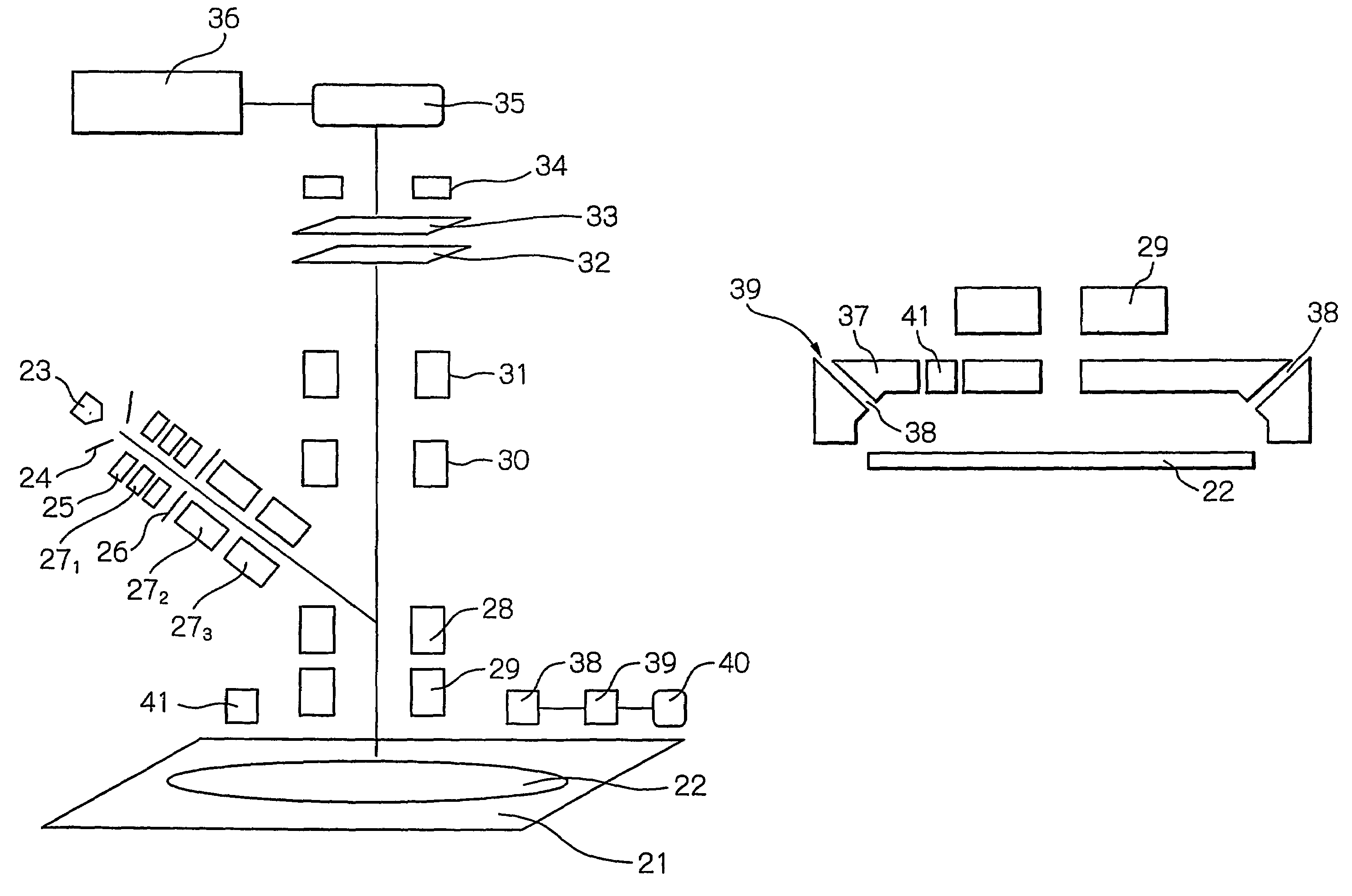
[0067]The entire sample chamber was evacuated with a turbomolecular pump to about 1.0E−5 Pa. A nitrogen gas was thereafter introduced from the nitrogen tank 40 into the cover 37 through the gas inlets 38 after reducing the pressure of the nitrogen gas to about 0.1 MPa by means of a regulator and adjusting a flow rate to 5 sccm with the flow rate controller 39. The introduced gas increased the pressure in the cover 37 to 4.0E−2 Pa, but such containers, for example, the electron gun chamber and the detector, that require high vacuum environment were maintained in a high vacuum state such as shown in FIG. 7 by a differential evacuation mechanism. In FIG. 7, MC indicates the gas pressure in the cover 37, EO indicates the gas pressure in the electron optical system chamber including E×B 28, MCP indicates the pressure in the chamber containing the detector including the MCP 32 and fluorescent screen 33.

[0068]Under such a pressure condition, the hot electron source 41 having a tungsten fil...

example 2

[0069]The same process as that in Example 1 was performed at a gas pressure higher than the gas pressure 0.1 Pa in Example 1 by introducing more nitrogen gas. Because the gas molecules came more frequently into contact with the sample 22, electric charge on the surface of the sample 22 was removed and the sample surface was positively charged. At a gas pressure lower than 0.01 Pa, the wafer continued to be negatively charged. In either case, it was revealed that a good image without any distortion was not obtained.

example 3

[0070]A halogen gas having higher affinity to electrons than nitrogen was introduced and the process in Example 1 was carried out. It was found that the time required for electric charge to be balanced on the surface of the sample 22 was reduced and that it was possible to enhance a throughput of inspection of a sample such as a wafer.


PUM

PropertyMeasurementUnit
energy levelaaaaaaaaaa
pressureaaaaaaaaaa
widthaaaaaaaaaa

Abstract

An apparatus capable of detecting defects of a pattern on a sample with high accuracy and reliability and at a high throughput, and a semiconductor manufacturing method using the same are provided. The electron beam apparatus is a mapping-projection-type electron beam apparatus for observing or evaluating a surface of the sample by irradiating the sample with a primary electron beam and forming on a detector an image of reflected electrons emitted from the sample. An electron impact-type detector such as an electron impact-type CCD or an electron impact-type TDI is used as the detector for detecting the reflected electrons. The reflected electrons are selectively detected from an energy difference between the reflected electrons and secondary electrons emitted from the sample. To eliminate charge-up caused on the sample surface by irradiation with the primary electron beam, the surface of the sample is covered with a cover placed above the sample and a gas is supplied to the space above the sample covered with the cover. The gas is brought into contact with the sample surface to reduce charge-up on the sample surface.

Description

TECHNICAL FIELD[0001]The present invention relates to an electron beam apparatus for performing inspection, observation and evaluation (electron beam testing) of the structure, electrical conduction, etc., of a sample surface by irradiating the sample surface with an electron beam and to an apparatus and method for inspecting defects on a pattern having a minimum line width of, for example, 0.15 μm or less with high accuracy and reliability and at a high throughput.BACKGROUND ART[0002]An inspection apparatus is known wherein a defect existing in a wafer is detected in such a manner that secondary electrons emitted when the surface of the substrate is irradiated and scanned with an electron beam are detected, wherein a wafer image data is produced on the basis of the detection result, and wherein the image data on each die on the wafer and the adjacent image data are compared with each other. A mapping-projection-type inspection apparatus is also well-known which obtains data on an i...

Claims


Application Information

Patent Timeline
Patent Type & Authority Patents(United States)
IPC IPC(8): H01J37/28G01N23/225H01J37/32
CPCG01N23/225H01J37/32211H01J37/32357H01J2237/2446H01J2237/2441
Inventor WATANABE, KENJIMURAKAMI, TAKESHIHATAKEYAMA, MASAHIROHIRABAYASHI, YOSHINAOSATAKE, TOHRUNOJI, NOBUHARUYAMAZAKI, YUICHIRONAGAHAMA, ICHIROTA
Owner TOSHIBA MEMORY CORP
Learn More