
Integrated circuit wafer packaging system and method

a technology of integrated circuit and packaging system, which is applied in the direction of packaging goods, furnaces, containers preventing decay, etc., can solve the problems of ic wafers not having the necessary features, scratching during the wafer insertion and transport process, and present-day transport media designed for packaging ic wafers lacking the necessary features, etc., to eliminate or seriously minimize the effect of corrosive amcs, eliminating or seriously minimizing the force caused by handling

Inactive Publication Date: 2009-08-25
CONVEY INC
View PDF11 Cites 30 Cited by
  • Summary
  • Abstract
  • Description
  • Claims
  • Application Information

AI Technical Summary

Benefits of technology

The CPS significantly reduces wafer damage during shipment by minimizing scratches, breakage, and corrosive contamination, enhancing product yields and ensuring the quality of bond pads and interconnects, while also promoting sustainable packaging practices through recycling.

Problems solved by technology

In general, present day transport media designed for packaging IC wafers are lacking the necessary features to address several problems common to advanced technology wafers during insertion and transport.
These problems can manifest themselves in the form of disfigured connectors that include wafer breakage, scratch damage as well as mobile ion induced parametric failures.
Wafer shipping containers / boxes in combination with bags, outer cardboard type boxes, cushions and separators that are not functionally coordinated nor objectively systematized to address wafer movement, Airborne Molecular Contaminants (AMCs), and vapor leakage during transport can cause yield problems to the semiconductor wafers.
The resulting wafer movement, when combined with wafers that utilize soft thin protective overcoats and elevated soft pads, caps and / or ground rings, can result in scratching during the wafer insertion and transport process.
Stacked wafers with elevated features may also transfer structural damage to other associated wafers if improper materials are selected with too soft or too stiff a compressibility factor.
Partial loading of a box changes the compressibility requirements of the system so that simply adding more cushions may not be the most appropriate solution.
These contaminates may lead to corrosive damage and / or transistor inversion.
AMCs are exceptionally small in size they are generally corrosive and they carry a charge.
Through molecular migration, a charge build may occur over an active transistor node resulting in transistor inversion and a parametric failure.
There will be no clear path leading back to the transport media system as a source of the problem.
The impact, depending on the weight of the wafer and the amount of trapped air, will result in some amount of uneven force as the two surfaces come in contact with each other.
The allowed lateral movement during the insertion will result in scratch damage.
Nor is it understood if this sub-micron crazing can later become a point of entry for corrosive growth.
It is known that such damage has been witnessed at the bevel edges of the wafers.
Scratch Damage: Smeared or Scratched Circuit Lead Scratches
During transport, lateral movement of wafers within containers / boxes will scratch wafer surfaces during shipment.
The resulting scratches will cause damage to interconnect circuitry including smashing and disfiguring elevated connecting members such as ground rings, ball bond pads, and caps.
The same lateral movement will also create shaving from the protective separators which further promotes scratch damage.
Wafers packaged within enclosures such as boxes and bags that have a high level of MVTRs (moisture vapor transport rate) when trapped within those enclosures that excessively out-gas Airborne Molecular Contaminants (AMCs), in combination can create corrosive residues that are able to settle on the surface.
Assuming no cracks or crazing have occurred to the passivation, the charge build that gathers above the transistor node may result in the transistor inverting, leading to a parametric circuit failure.
Generally these AMCs have already attached themselves to the oxide so that saw and grind slurry and their respective cleanups accomplish little to achieve removal.
For wafers packaged within shipping containers, there are instances where bond pads and adjacent passivation coatings will accumulate contamination that appears as a stain.
Clean rooms are teeming with AMCs that cannot be effectively removed by HEPA filters.
A small amount of chemical reaction takes place with the exposed aluminum or copper surface, thereby resulting in a corrosive stain in the area of bond pads as well as in any area where a mismatch between the photo-resist and the PO coating occurs.
Surfaces of bond pads that become excessively corroded while in transit from one location to another may become unnecessarily exposed to the condition of AMCs.
This damage is normally restricted to bond pad surfaces only and normally is associated with the presence of moisture vapors.
This out-gassing may be linked to inorganic and organic type AMCs resulting in the corrosive damage.

Method used


Image

  • Integrated circuit wafer packaging system and method
  • Integrated circuit wafer packaging system and method
  • Integrated circuit wafer packaging system and method

Examples


Embodiment Construction

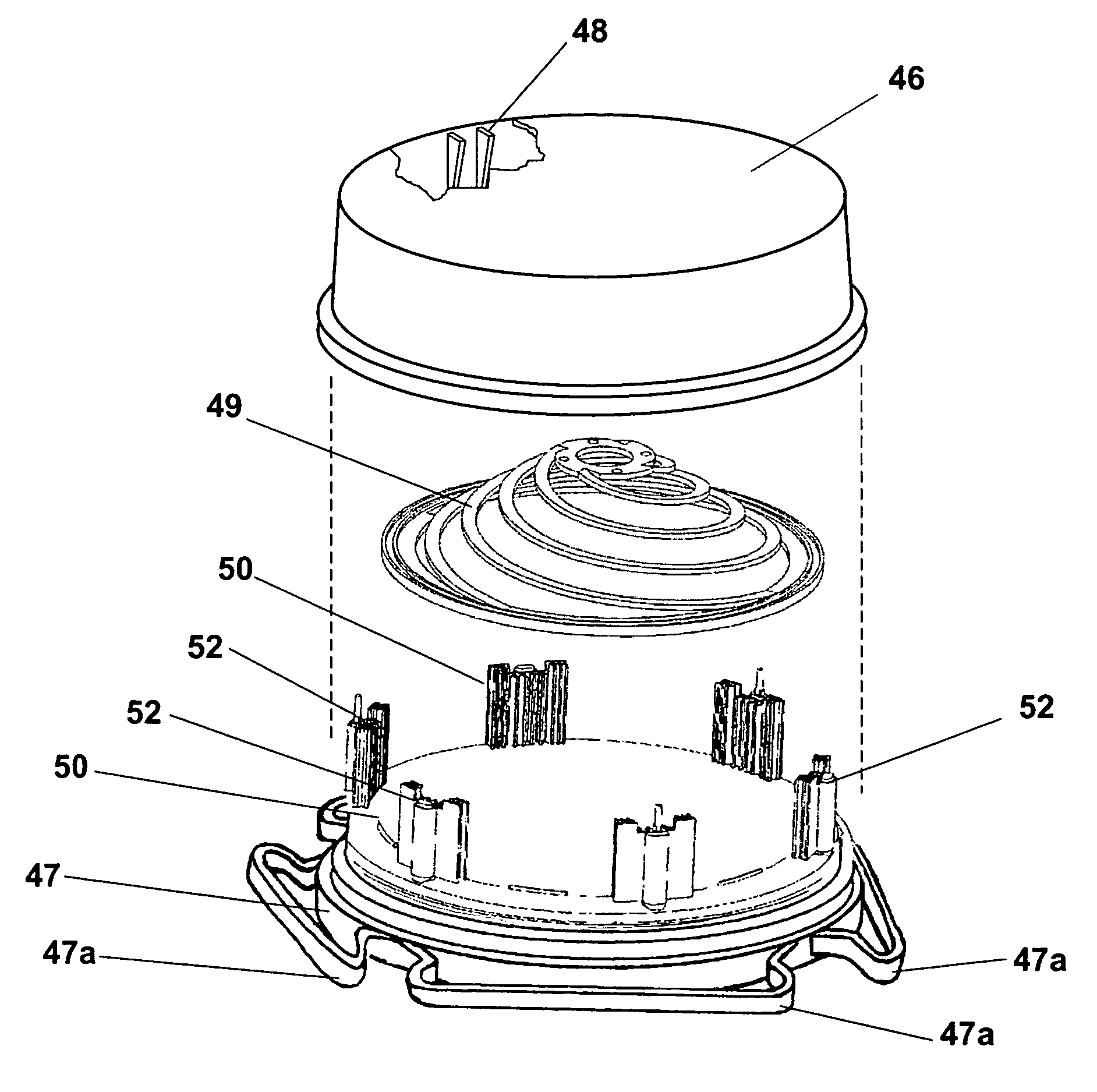
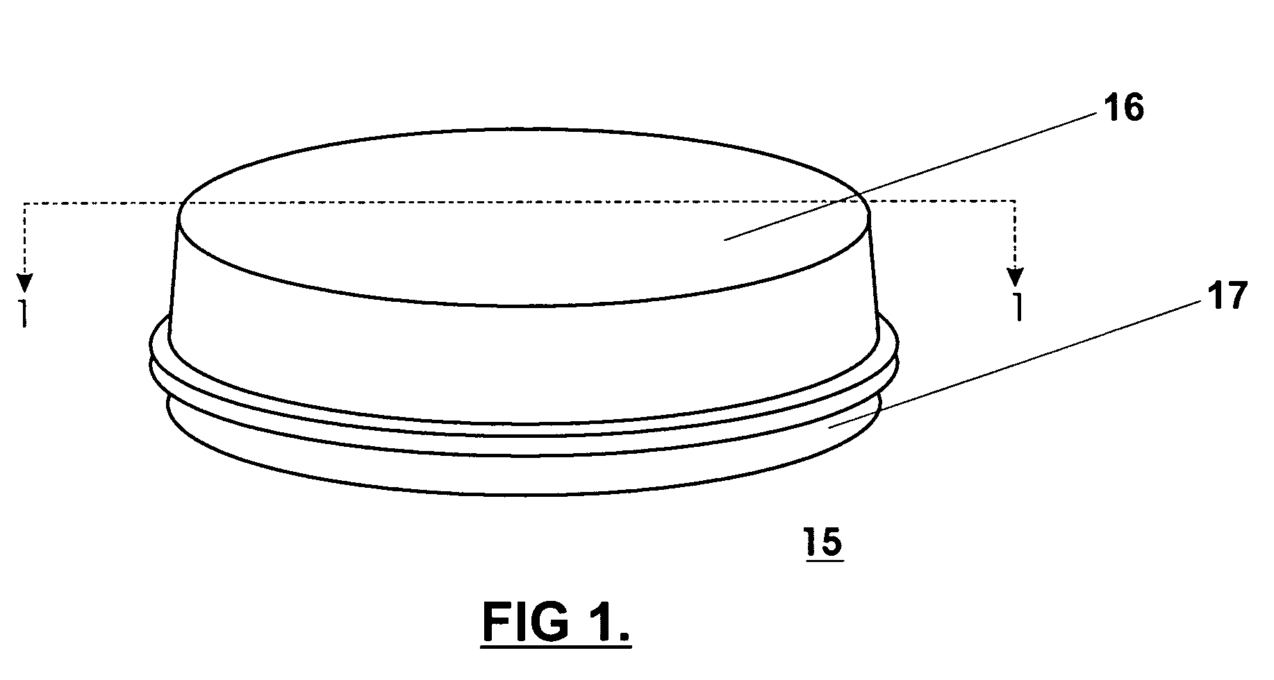
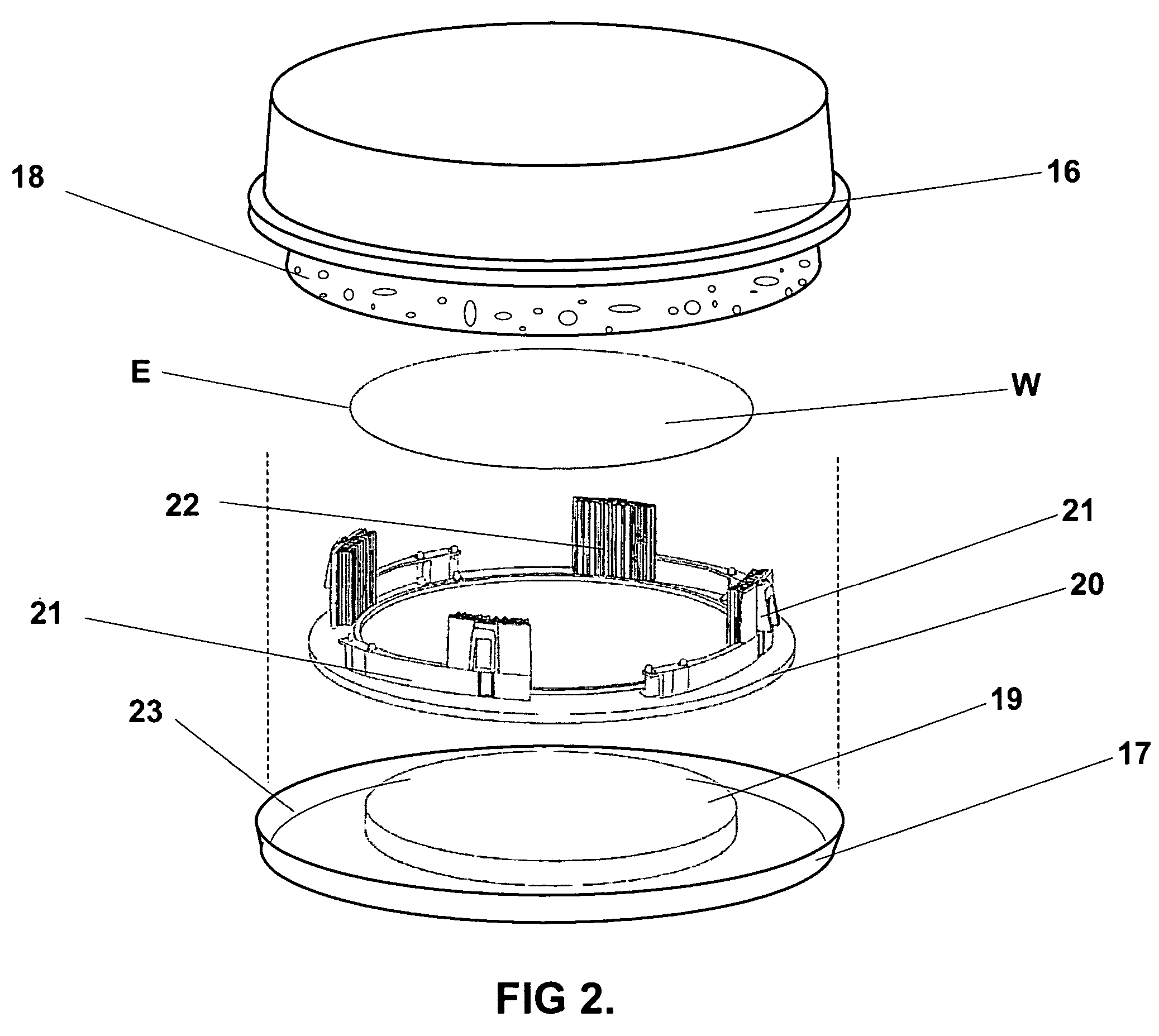
[0076]The invention is a container for shipping and / or storing semiconductor wafers to prevent damage to the wafers. A first embodiment of the invention is illustrated in FIGS. 1, 2, 3, and 4. The box or container is referred to as WEC (Wafer Environmental Control) Box that is designed to comply with all the features of the CP System. The box / container is molded of a synthetic resinous material such as ABS and is designed in a manner to accommodate and resolve critical issues such as contaminating Airborne Molecular Contaminants, directional forces during shipment phases that create motion for packaged wafers that cause surface damage and means to absorb shock energy caused by mishandling, all of which occur during shipment phase.

[0077]FIG. 1 is an isometric view of an embodiment of the invention. FIG. 1 shows a Box / container 15 with a top cover 16 and a bottom cover 17.

[0078]FIG. 2 is an exploded view of box 15, showing the basic components of the box / container. There is a bottom c...


PUM


Abstract

A packaging system, hereinafter referred to as the Critical Packaging System, relates to critical issues that associate with sensitive articles such as IC wafers before, during and after shipment phases. The system employs a choice of two or more specialty designed containers, and any one selected design having choices of two or more methods by which to avoid, reduce and / or eliminate wafer damage from breakage, scratches and / or corrosion during shipment phases. For the purpose of maximizing product yield during packaging phases a special apparatus is used to insert wafers within containers without scratch damage. The following programs are used in packaging: (1) Quality Assurance / Certification, (2) Critical Factor Monitoring, and (3) a Recycle and Refurbish Program. These programs are specifically designed to achieve new levels of product yields, reduce product cost, and landfill impact.

Description

[0001]This application claims the benefit of U.S. provisional application Ser. No. 60 / 476,790, filed Jun. 6, 2003.FIELD OF THE INVENTION[0002]The invention relates to semiconductor wafer packaging and transportation system, and more particularly to a packaging system and method of packaging sensitive articles such as semiconductor wafers to prevent damage to the wafers before, during and after storage / shipment phases.BACKGROUND OF THE INVENTION[0003]To date, the semiconductor industry has been able to produce IC wafers increasing functional capabilities and increasing density without necessarily suffering losses during the transport processes, or at least having not realized the packaging media as a source for those losses. In general, present day transport media designed for packaging IC wafers are lacking the necessary features to address several problems common to advanced technology wafers during insertion and transport. This is especially true for wafers having higher speed wit...

Claims


Application Information

Patent Timeline
Patent Type & Authority Patents(United States)
IPC IPC(8): B65D85/30B65D57/00B65D21/02B65D81/07B65D81/26B65D85/86B65G49/07H01L21/673H01L21/677H01L21/68
CPCH01L21/67353H01L21/67369H01L21/67386H01L21/67373Y10S206/832H01L21/68
Inventor BROOKSBROOKS, TIMOTHY W.
Owner CONVEY INC
Learn More