
Clock driver

a technology of clock driver and driver, which is applied in the direction of generating/distributing signals, pulse techniques, instruments, etc., can solve the problems of increasing power consumption, reducing power consumption is a big problem, and the threshold voltage of transistors is not always changed, so as to achieve excellent charge recycling efficiency and reduce the occupation area

Active Publication Date: 2009-04-21
SK HYNIX INC
View PDF18 Cites 33 Cited by
  • Summary
  • Abstract
  • Description
  • Claims
  • Application Information

AI Technical Summary

Benefits of technology

The present invention provides a clock driver that can improve charge recycling efficiency and reduce the occupation area. It achieves this by selectively transferring an input clock signal to the charge recycling switch based on the first and second pumping clock signals. The charge recycling switch may be a NMOS or PMOS transistor, and the switch controller may be a transmission gate or an XOR / XNOR gate. The clock driver may include a plurality of inverter chains and can improve charge recycling time while implementing a reduced logic configuration.

Problems solved by technology

As semiconductor memory devices are integrated more highly, their power consumption also increases.
Therefore, the reduction of the power consumption is a big issue in the highly integrated semiconductor memory devices.
However, threshold voltages of transistors are not always changed even though the semiconductor memory devices are highly integrated.
Also, even if the power consumption used in charging or discharging the capacitors is excluded, much current loss occurs in the inverter chains during a transient period in which the logic level is changed.
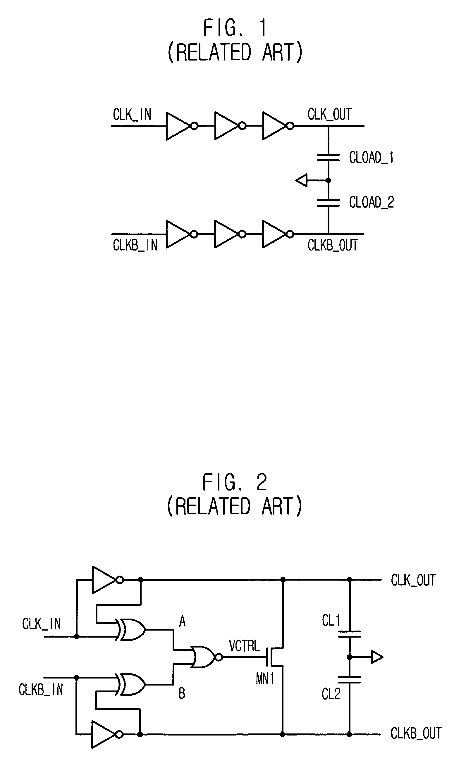
In such a clock driver, when the signal is changed, electric charges in the capacitors are all discharged through an NMOS transistor disposed in a last stage of the inverter, thus exhibiting the low power efficiency.
According to the charge-recycling method, however, the driving of the charge recycling consumes much power when the structure is complicated or the area is too large.
Therefore, the control voltage has a predetermined delay.
Although the author of the paper does not specify the concrete scheme of the XOR gate or NOR gate, a considerable delay may occur in the worst case, considering the typical structure of the XOR gate or NOR gate.

Method used


Image

  • Clock driver
  • Clock driver
  • Clock driver

Examples


Embodiment Construction

[0061]A clock driver in accordance with exemplary embodiments of the present invention will be described in detail with reference to the accompanying drawings.

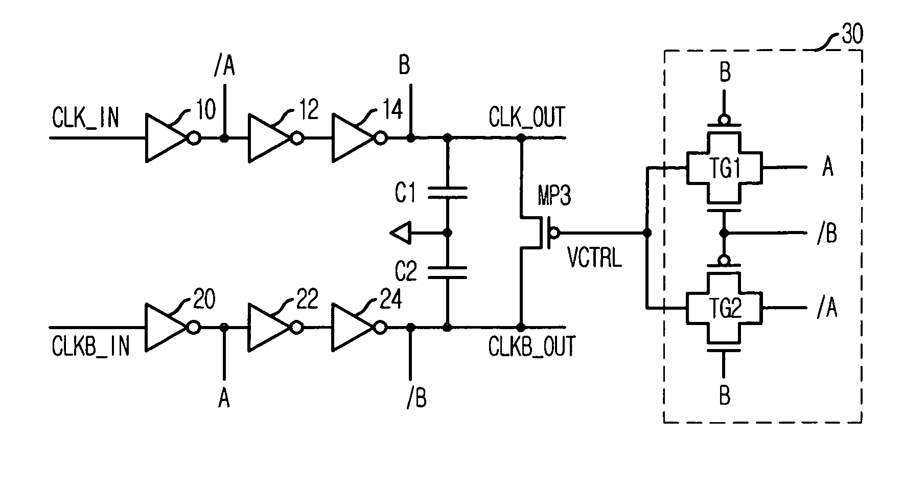
[0062]FIG. 5 is a circuit diagram of a clock driver in accordance with an embodiment of the present invention.

[0063]Referring to FIG. 5, the clock driver includes a first clock-first driver 10, a first clock-second driver 12, a first clock-third driver 14, a second clock-first driver 20, a second clock-second driver 22, a second clock-third driver 24, a charge recycling switch MP3, a switch controller 30, and first and second capacitors C1 and C2.

[0064]The first clock-first driver 10 receives a first clock signal CLK_IN, the first clock-second driver 12 is connected to an output terminal of the first clock-first driver 10, and the first clock-third driver 14 is connected to an output terminal of the first clock-second driver 12 to output a first pumping clock CLK_OUT. The second clock-first driver 20 receives a second clock si...


PUM


Abstract

A clock driver is provided. A first driving unit is configured with a plurality of drivers and receives a first clock signal to drive a first pumping clock. A second driving unit is configured with a plurality of drivers and receives a second clock signal to drive a second pumping clock. A charge recycling switch is connected between an output terminal of the first driving unit and an output terminal of the second driving unit. A switch controller selectively transfers an input clock signal of the first or second driving unit to the charge recycling switch in response to the first and second pumping clock signals.

Description

FIELD OF THE INVENTION[0001]The present invention relates to a semiconductor memory device; and, more particularly, to a clock driver with low power consumption to control a large-capacity load capacitor.DESCRIPTION OF RELATED ART[0002]As semiconductor memory devices are integrated more highly, their power consumption also increases. Therefore, the reduction of the power consumption is a big issue in the highly integrated semiconductor memory devices.[0003]A power supply voltage used in the semiconductor memory device is closely associated with power consumption. That is, the reduction of the power supply voltage results in the reduction of the power consumption. However, threshold voltages of transistors are not always changed even though the semiconductor memory devices are highly integrated. Thus, a voltage higher than the power supply voltage, i.e., a high voltage VPP, has to be applied to a word line so as to access a selected memory cell. For this purpose, a VPP pumping circui...

Claims


Application Information

Patent Timeline
Patent Type & Authority Patents(United States)
IPC IPC(8): G06F1/04
CPCG06F1/10G11C5/145G11C7/222H03K19/0175
Inventor KIM, DONG-HWANKIM, SI-NAEKWACK, KAE-DALLEE, JAE-JIN
Owner SK HYNIX INC
Learn More