Liquid crystal panel, liquid crystal display device, and electronic equipment
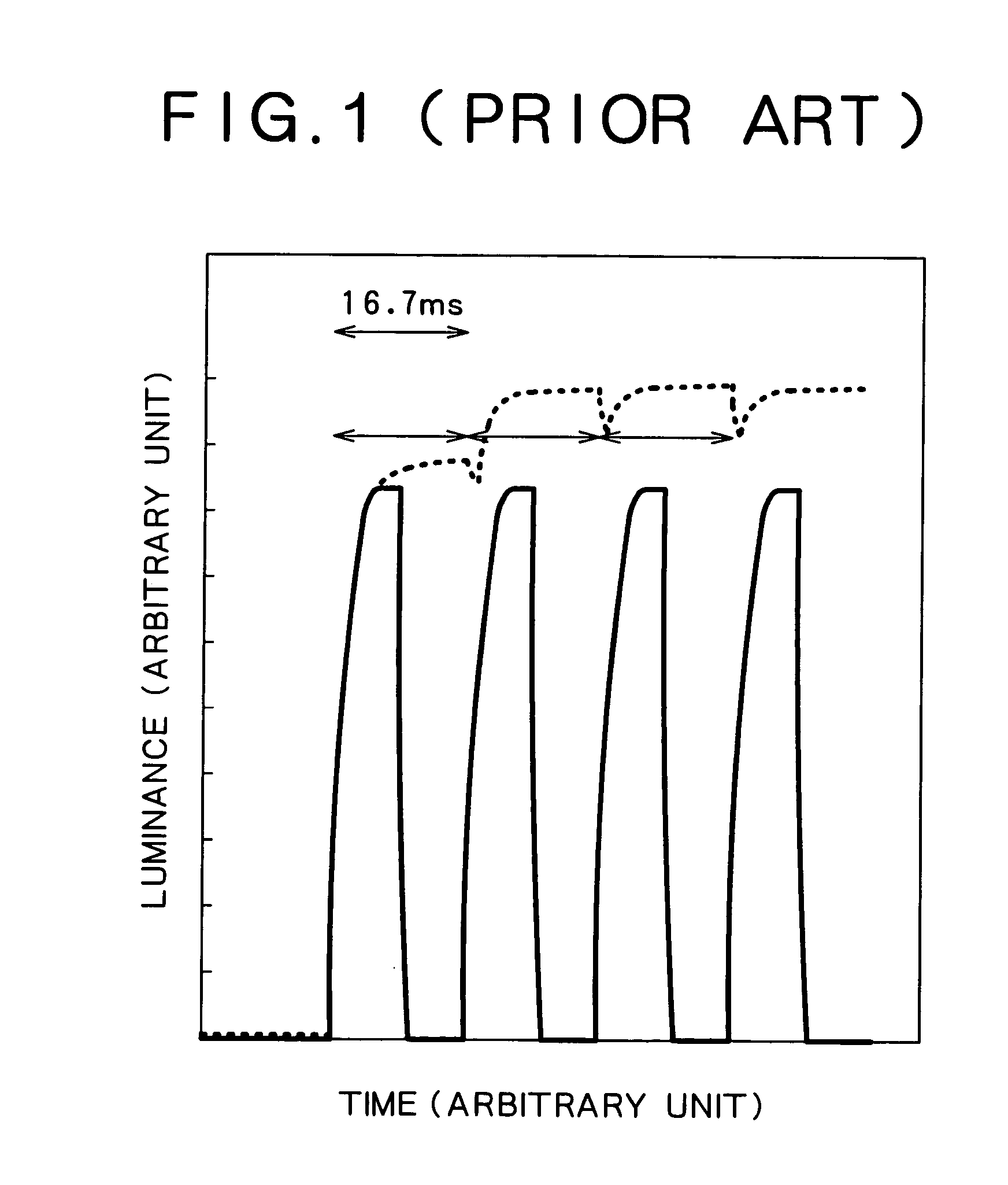
a liquid crystal display and liquid crystal technology, applied in liquid crystal compositions, instruments, chemistry apparatus and processes, etc., can solve the problems of low display quality, stn mode is not suitable for motion image display, stn mode, etc., to increase the response speed of the liquid crystal at decay time, increase the response speed of the liquid crystal, and increase the response speed of the twisted nematic liquid crystal
- Summary
- Abstract
- Description
- Claims
- Application Information
AI Technical Summary
Benefits of technology
Problems solved by technology
Method used
Image
Examples
first embodiment
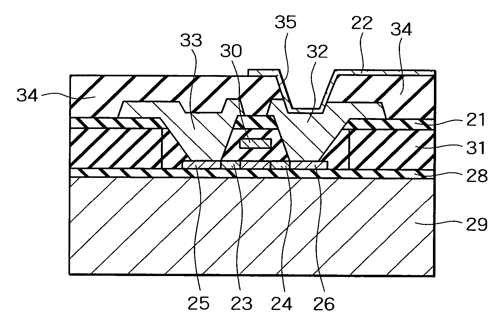
[0093]Embodiments of the present invention will be described below in detail with reference to the accompanying drawings. Now, the present invention will be described. FIG. 6 is a cross-sectional view showing a unit structure of a TFT array in a liquid crystal panel according to the embodiment of the present invention. The TFT array shown in FIG. 6 is a polysilicon TFT array, which is formed by modifying amorphous silicon into polysilicon.
[0094]As shown in FIG. 6, the polysilicon TFT has a structure in which a silicon oxide film 28 is formed on a glass substrate 29 and a polysilicon layer is locally formed thereon. This polysilicon layer is formed by depositing amorphous silicon on the silicon oxide layer 28, then modifying the amorphous silicon into polysilicon by annealing with an excimer laser, and then patterning the polysilicon. A gate oxide film is formed in a thickness of 10 nm on a surface of this polysilicon layer. In FIG. 6, the gate oxide film corresponds to a lower porti...
second embodiment
[0138]In the second embodiment, it is preferable that the light shielding film is formed on the TFT substrate. The reason is as follows. Upon polymerization by the light irradiation, the light is irradiated from the counter electrode side. The light loss is significant on the TFT substrate side because the TFTS, the pixel electrodes, the wiring, and the like are formed thereon, and it is therefore difficult to irradiate the light uniformly to the monomer. In this way, the light irradiation is not performed from the TFT array substrate side. When the light shielding film is formed on the opposite substrate, unreacted monomer remains in the portions shielded by the light shielding film after the light irradiation. When the unreacted monomer remains therein, the unreacted monomer may cause a problem such as interference with the alignment of the liquid crystal which is attributable to subsequent polymerization of the unreacted monomer by outside light while the state of alignment of th...
PUM
| Property | Measurement | Unit |
|---|---|---|
| pretilt angle | aaaaa | aaaaa |
| pretilt angle | aaaaa | aaaaa |
| time | aaaaa | aaaaa |
Abstract
Description
Claims
Application Information
 - R&D
- Intellectual Property
- Life Sciences
- Materials
- Tech Scout
- Unparalleled Data Quality
- Higher Quality Content
- 60% Fewer Hallucinations
Browse by: Latest US Patents, China's latest patents, Technical Efficacy Thesaurus, Application Domain, Technology Topic, Popular Technical Reports.
© 2025 PatSnap. All rights reserved.Legal|Privacy policy|Modern Slavery Act Transparency Statement|Sitemap|About US| Contact US: help@patsnap.com


