
Electronic isolator

a technology of isolators and electrical signals, applied in the field of electronic isolators, can solve the problems of low signal attenuation, large cost, and large size of relatively narrow band devices (10%-20% being typical), and achieve the effects of high signal attenuation, low signal attenuation, and high asymmetric attenuation of electrical signals

Inactive Publication Date: 2008-09-02
MASHHOON HAMID R
View PDF28 Cites 8 Cited by
  • Summary
  • Abstract
  • Description
  • Claims
  • Application Information

AI Technical Summary

Benefits of technology

The solution achieves high asymmetry in signal attenuation with low insertion loss and wideband operation, enabling smaller, lighter, and less expensive isolators that can be integrated into low-power applications without the limitations of prior art.

Problems solved by technology

However, currently available isolators suffer from a number of disadvantages.
These solutions all have significant limitations in performance and applicability.
The result is a relatively narrow band device (10%-20% being typical) that is relatively large and costly.
As a result, the use of magnetic isolators is typically restricted to certain applications where the size can be accommodated, such as test equipment and the interface between high power amplifiers and antennas being the principle applications.
It relies on the constructive and destructive interference of signals to produce low insertion loss and high isolation effects.
The signals destructively interfere at the input port as they continue to propagate around the circuit or are reflected off the output port.
Similarly, it is possible to locate a point(s) where a signal injected at the output port constructively interferes while at the same time the same signal injected at the input destructively interferes.
A disadvantage of the rat race approach is that as an interference system, it is inherently narrow band.
The second problem is that the path length of the closed loop must be a significant portion of a wavelength.
Thus, even at microwave frequencies, the path may be too long to be practical.
It is certainly much too long to be incorporated into an integrated circuit much below W-band.
This additional power requirement may be too expensive to achieve or may unduly limit circuit performance.
As a result, the use of isolation pads is usually limited to low power circuits and compensation for the loss is achieved by added gain stages, or added gain and power from the down stream circuitry, an expensive and complicated solution.

Method used


Image

  • Electronic isolator
  • Electronic isolator
  • Electronic isolator

Examples


Embodiment Construction

[0036]The present invention is directed to an electronic isolator. In the following description, numerous specific details are set forth to provide a more thorough description of embodiments of the invention. It is apparent, however, to one skilled in the art, that the invention may be practiced without these specific details. In other instances, well known features have not been described in detail so as not to obscure the invention.

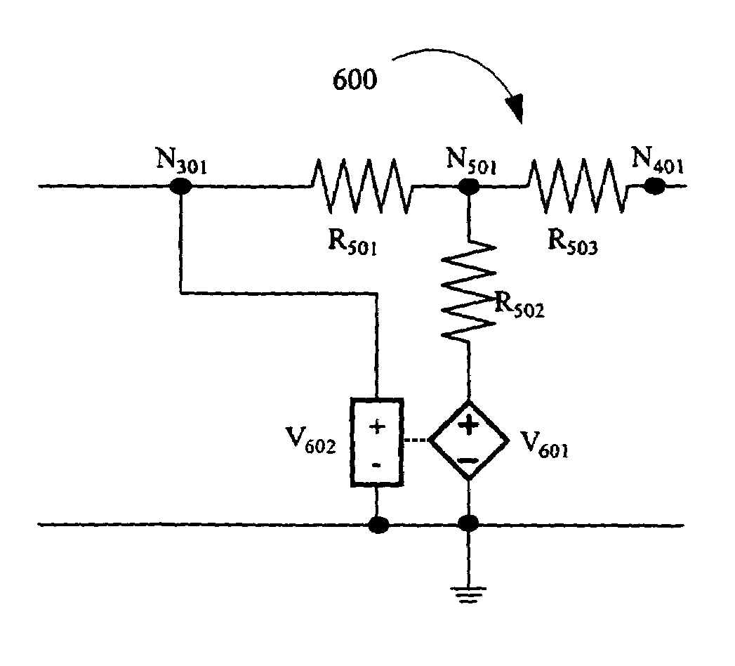
[0037]The present invention enables electronic circuit designers to realize the classic isolation function with an electronic circuit design as opposed to a non-linear physical process. This invention differentiates the source signal from the source signal plus noise reflected from the load. This noise may include out-of-phase source signal or harmonic distortion induced by a nonlinear device such as a diode or transistor. This invention uses no magnets or magnetic materials. It is not wavelength sensitive and as such is wideband with no significant fre...


PUM


Abstract

The present invention is an electronic isolator that provides low input to output insertion loss, high output to input insertion loss, and substantial asymmetric isolation between a source circuit and a load circuit. The invention actively reduces noise and reflected power appearing on the isolator output. In numerous embodiments, the invention operates in circuit applications from dc through millimeter wave. Multistage electronic isolator embodiments provide increased isolation and greater noise reduction. In other embodiments, the electronic isolator also removes noise appearing on its input. In another embodiment, the invention is configured for high power applications. This embodiment includes circuitry for redirecting power away from the load into resistors or other dissipative elements. In another embodiment, the electronic isolator is configured to remove signal distortion produced by one or more power amplifiers in the system.

Description

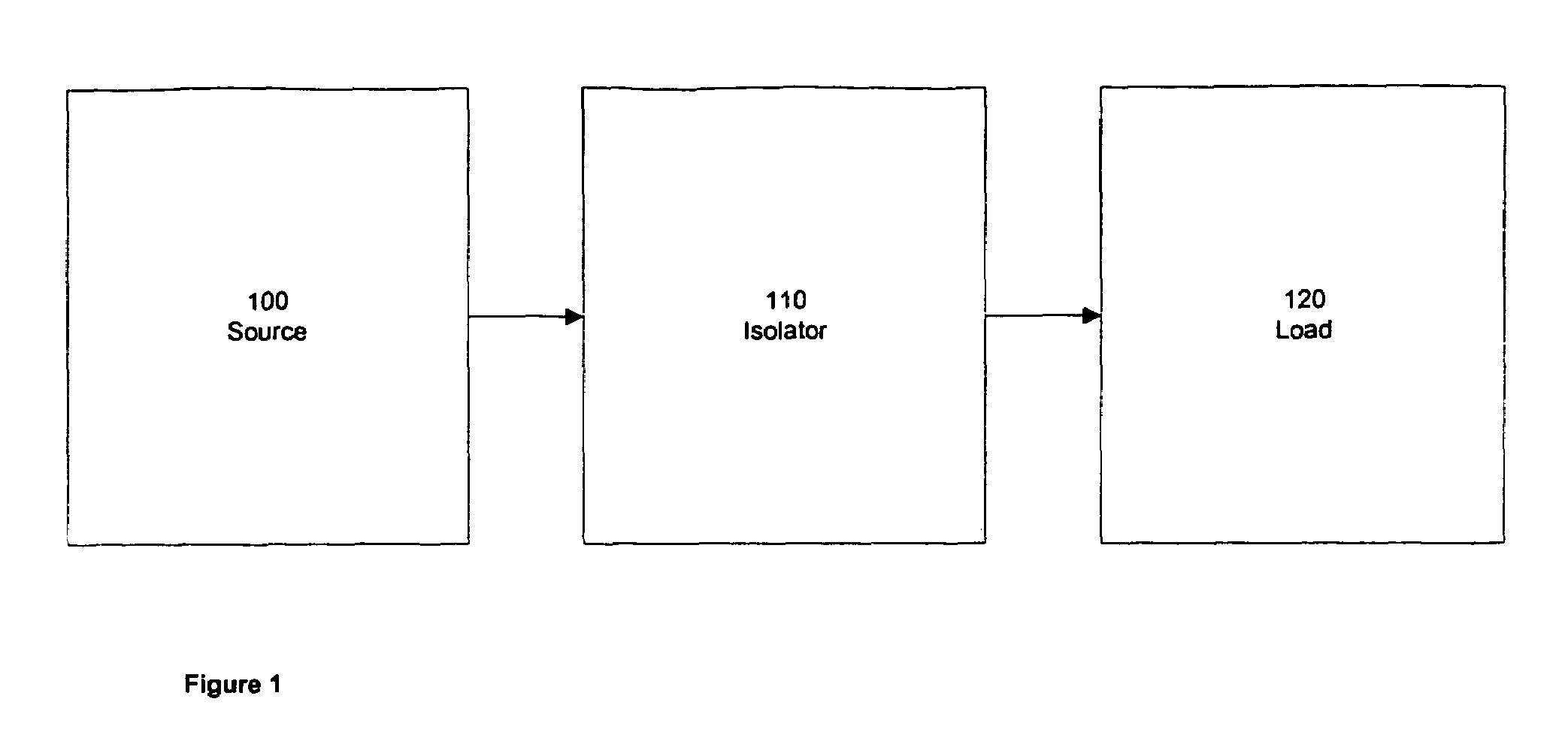
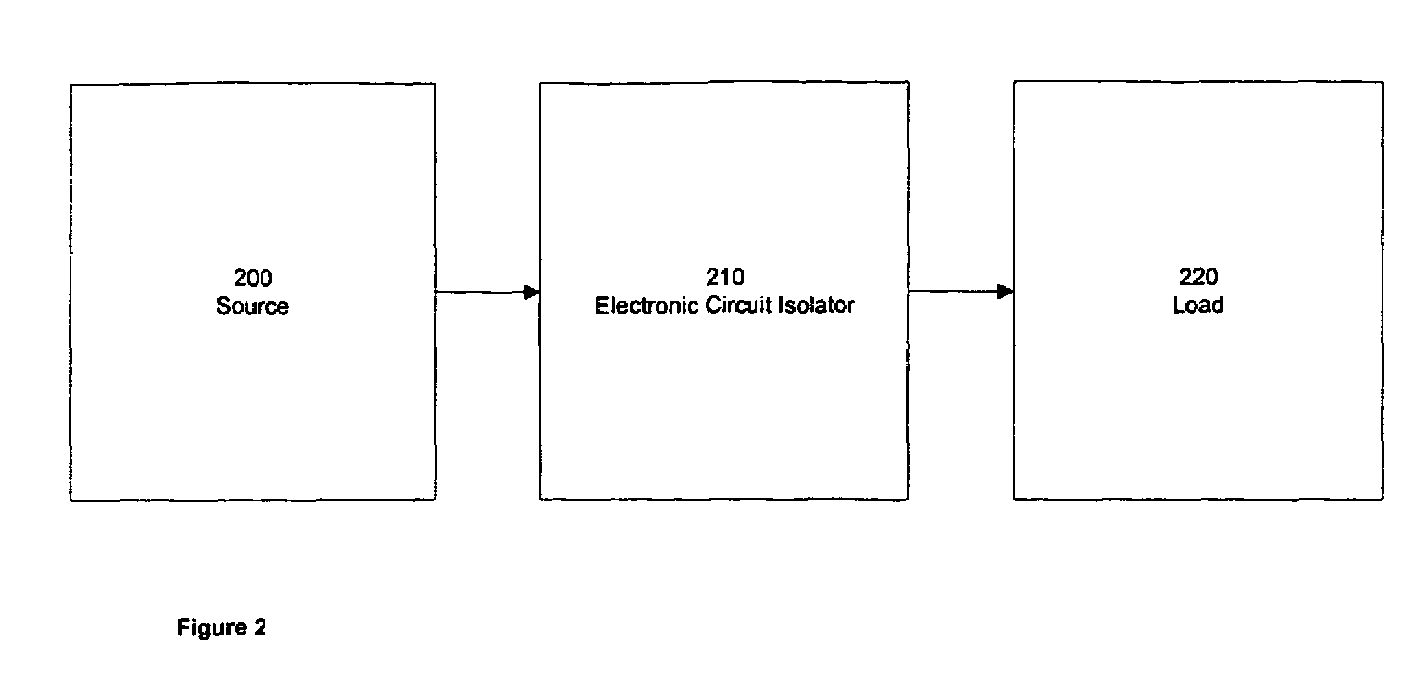
CROSS-REFERENCE TO RELATED APPLICATIONS[0001]This is a divisional of U.S. patent application Ser. No. 09 / 866,563, filed May 25, 2001, now U.S. Pat. No. 6,897,704.BACKGROUND OF THE INVENTION[0002]1. Field of the Invention[0003]The present invention relates to the field of electronic isolators.[0004]2. Background Art[0005]Electronic circuits are often made up of a number of discrete “stages” where the output of a first stage is provided as input to a subsequent second stage. To maximize performance, it is sometimes desired to provide isolation between the stages, so that the operation of the first stage is not affected by the operation of the second stage. Generally, this has been accomplished by employing an isolator between the circuit stages. However, currently available isolators suffer from a number of disadvantages.[0006]Referring to FIG. 1, a multistage circuit is symbolically indicated. The circuit consists of a source stage 100 that provides output to a load stage 120. The so...

Claims


Application Information

Patent Timeline
Patent Type & Authority Patents(United States)
IPC IPC(8): H03L5/00H03F1/56H03H7/52H03H11/38
CPCH03F3/45475H03H7/52H03H11/38H03F2200/168H03F2203/45138H03H11/48H03F2203/45528
Inventor WASHBURN, ROBERT D.MCCLANHAN, ROBERT F.
Owner MASHHOON HAMID R
Learn More