
Compound semiconductor multilayer structure, hall device, and hall device manufacturing method

a multi-layer structure and compound semiconductor technology, applied in the direction of galvano-magnetic hall-effect devices, instruments, galvano-magnetic devices, etc., can solve the problems of large mismatching between crystal lattice spacings in substrates, degradation of crystallinity and mobility, etc., to achieve high mobility characteristics, ease the mismatch, and high resistance

Inactive Publication Date: 2008-06-17
ASAHI KASEI ELECTRONICS CO LTD
View PDF48 Cites 0 Cited by
  • Summary
  • Abstract
  • Description
  • Claims
  • Application Information

AI Technical Summary

Benefits of technology

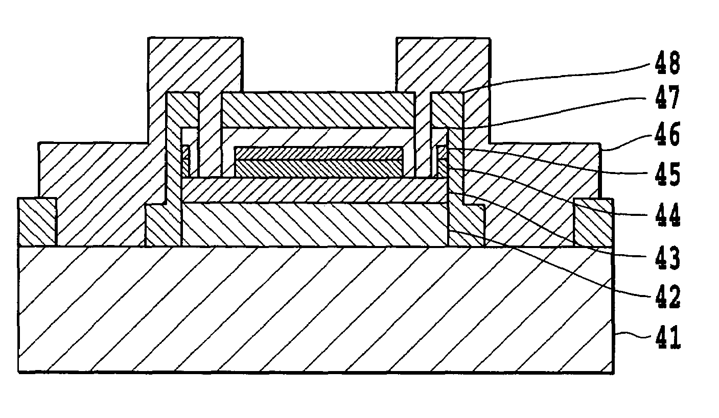
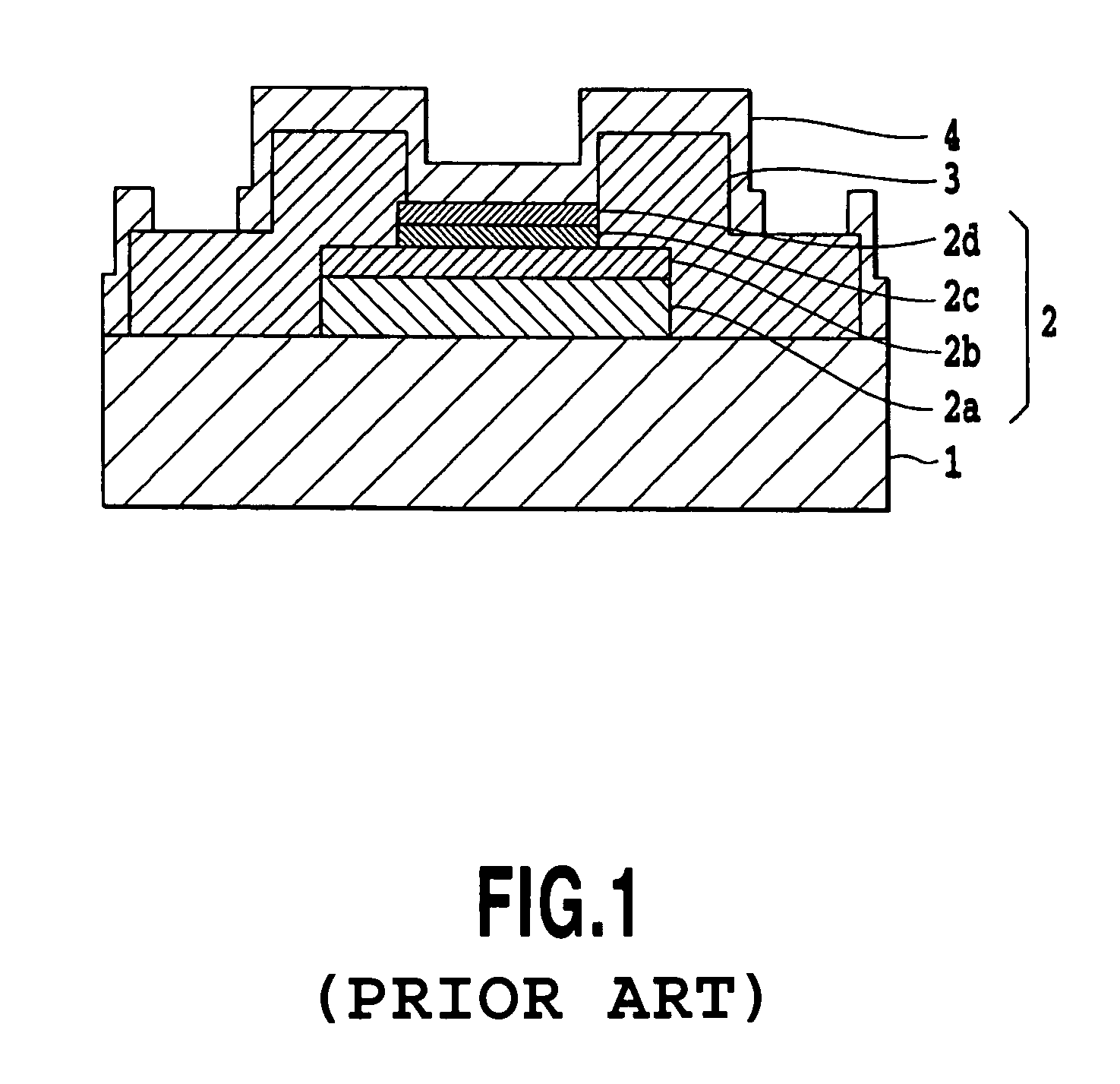
The present invention relates to a method for fabricating a low power consumption, highly sensitive Hall device with good temperature characteristics. The technical effects of the invention include the use of a high resistance, high mobility semiconductor thin film to achieve both high resistance and high sensitivity, the formation of a thin active layer with good crystallogy to maintain its crystallinity, the use of a multilayer structure to ease the lattice mismatch between the substrate and the active layer, the use of a passivation process to cover all surfaces of the semiconductor layers to reduce variations in the device, the use of a cap layer with good soldering heat resistance to stabilize the interface conditions, and the use of a compound semiconductor with a composition that matches the active layer for the magneto-sensitive pattern. The invention also provides a compound semiconductor stacked structure and a Hall device comprising the semiconductor thin films and compound semiconductor layers.

Problems solved by technology

The Hall devices up to now have a problem in that the thin active layers bring about degradation in the crystallinity and reduction in the mobility.
This is because since the active layers are formed immediately on the substrates, large mismatching occurs between crystal lattice spacings in the substrates and the active layers.

Method used


Image

  • Compound semiconductor multilayer structure, hall device, and hall device manufacturing method
  • Compound semiconductor multilayer structure, hall device, and hall device manufacturing method
  • Compound semiconductor multilayer structure, hall device, and hall device manufacturing method

Examples


example 1

[0140]On a GaAs substrate two inches in diameter, are successively formed by the molecular beam epitaxy (MBE) 600 nm Al0.55Ga0.45AsSb as the first compound semiconductor layer, 50 nm InAs as the active layer, 60 nm Al0.55Ga0.45AsSb as the second compound semiconductor layer, and 6 nm GaAsSb as the third compound semiconductor layer.

[0141]The Sb composition was calculated, according to Vegard's law, from accurate lattice constants obtained by a high resolution X-ray diffraction method based on a 4-crystal method using Ge (220) single crystals. The electric characteristics such as the electron mobility were evaluated from the measurement of the Hall effect by van der Pauw method.

[0142]Table 2 summarizes the thus obtained lattice constant difference, electron mobility and sheet resistance in accordance with the Sb compositions.

[0143]

TABLE 2latticeconstantelectronsheetdifferencemobilityresistanceSbx(%)(cm2 / Vs)(Ω)0.8850.10191125280.9020.23197054770.9180.35206014280.9290.43213043990.9380....

example 2

[0155]On a GaAs substrate two inches in diameter, are successively formed by the molecular beam epitaxy (MBE) 600 nm Al0.55Ga0.45AsSb as the first compound semiconductor layer, 70 nm InAs as the active layer, 60 nm Al0.55Ga0.45AsSb as the second compound semiconductor layer, and 6 nm GaAsSb as the third compound semiconductor layer.

[0156]The Sb composition was calculated, according to Vegard's law, from accurate lattice constants obtained by the high resolution X-ray diffraction method based on the 4-crystal method using Ge (220) single crystals. The electric characteristics such as the electron mobility were evaluated from the measurement of the Hall effect by van der Pauw method.

[0157]Table 4 summarizes the thus obtained lattice constant difference, electron mobility and sheet resistance in accordance with the Sb compositions.

[0158]

TABLE 4latticeconstantelectronsheetdifferencemobilityresistanceSbx(%)(cm2 / Vs)(Ω)0.8860.11165695350.9010.22173524910.9190.36188094340.9370.49201043900.9...

example 3

[0161]On a GaAs substrate two inches in diameter, are successively formed by the molecular beam epitaxy (MBE) 600 nm Al0.55Ga0.45AsSb as the first compound semiconductor layer, 35 nm InAs as the active layer, 60 nm Al0.55Ga0.45AsSb as the second compound semiconductor layer, and 6 nm GaAsSb as the third compound semiconductor layer.

[0162]The Sb composition was calculated, according to Vegard's law, from accurate lattice constants obtained by the high resolution X-ray diffraction method based on the 4-crystal method using Ge (220) single crystals. The electric characteristics such as the electron mobility were evaluated from the measurement of the Hall effect by van der Pauw method.

[0163]Table 5 summarizes the thus obtained lattice constant difference, electron mobility and sheet resistance in accordance with the Sb compositions.

[0164]

TABLE 5latticeconstantelectronsheetdifferencemobilityresistanceSbx(%)(cm2 / Vs)(Ω)0.8920.15196057430.9040.24205186560.9180.35216735900.9340.47228455210.9...


PUM


Abstract

Hall device is provided by enabling stable provision of a quantum well compound semiconductor stacked structure. It has first and second compound semiconductor layers composed of Sb and at least two of five elements of Al, Ga, In, As and P, and an active layer composed of InxGa1-xAsySb1-y (0.8≦x≦1.0, 0.8≦y≦1.0), which are stacked. Compared with the active layer, the first and second compound semiconductor layers each have a wider band gap, and a resistance value five times or more greater. The lattice constant differences between the active layer and the first and second compound semiconductor layers are each designed in a range of 0.0-1.2%, and the thickness of the active layer is designed in a range of 30-100 nm.

Description

TECHNICAL FIELD[0001]The present invention relates to a compound semiconductor stacked structure and a compound semiconductor Hall device using the structure, and their fabrication method. More specifically, the present invention relates to a stacked compound semiconductor Hall device with an active layer of InAs or the like, and aims to provide a highly sensitive, low power consumption magnetic sensor with excellent temperature characteristics using a stacked structure, which is a quantum well compound semiconductor stacked structure with high electron mobility and sheet resistance, and excellent temperature characteristics.[0002]In addition, the present invention relates to various devices for mobile equipment using the Hall device.BACKGROUND ART[0003]Generally, Hall devices are used for the rotation control and position detection of motors and for magnetic field detection, and find extensive application in such fields as brushless motor, noncontact open / close detection switch, an...

Claims


Application Information

Patent Timeline
Patent Type & Authority Patents(United States)
IPC IPC(8): H01L43/00G01R33/07H01L29/201H01L29/205H10N52/00H10N52/01
CPCG01R33/07H01L29/201H01L29/205H01L43/065H01L43/14H10N52/101H10N52/01H01L29/778H10N52/00
Inventor WATANABE, TAKAYUKISHIBATA, YOSHIHIKOUJIHARA, TSUYOSHIYOSHIDA, TAKASHIOYAMA, AKIHIKO
Owner ASAHI KASEI ELECTRONICS CO LTD
Learn More