Method of fabricating a MIS transistor

Inactive Publication Date: 2008-04-01
SEMICON ENERGY LAB CO LTD
View PDF114 Cites 0 Cited by
  • Summary
  • Abstract
  • Description
  • Claims
  • Application Information

AI Technical Summary

Benefits of technology

[0011]In view of the foregoing problems, the present invention has been made. It is an object of the present invention to provide a method of efficiently carrying out an activation step using laser illumination.
[0014]It is another object of the invention to provide a method of efficiently carrying out an implantation step and a laser activation step.
[0015]In one embodiment of the present invention, an insulating film is formed as a gate-insulating film. Impurity ions are implanted into a semiconductor region through all or parts of the insulating film by irradiation of high-speed ions. Then, the insulating film is removed excluding the portions located under the gate electrode portions, thus exposing the semiconductor region. Laser light or other equivalent intense light is illuminated to perform an anneal. The above-described absorption of light by the insulating film does not take place. Activation can be done quite efficiently.
[0016]In another embodiment of the invention, a first insulating film is formed as a gate-insulating film. Using the gate electrode portions as a mask, the first insulating film is removed by a self-aligning process to expose the semiconductor surface. Then, impurity ions are implanted into the exposed semiconductor layer by irradiation of high-speed ions. Thereafter, a second insulating film of an appropriate thickness is formed on the exposed semiconductor layer. Thereafter, the semiconductor layer is irradiated with laser light or equivalent intense light through the second insulating film to perform an anneal. In this method, the above-described deterioration in the implantation efficiency is prevented. Rather, an ion implantation step and a subsequent activation step can be accomplished quite efficiently.
[0017]In a further embodiment of the invention, a first insulating film is formed as a gate-insulating film. Using the gate electrode portions as a mask, the first insulating film is removed by a self-aligning process to expose the semiconductor layer surface. Then, a second insulating film of an appropriate thickness is formed on the semiconductor layer. Impurity ions are implanted into the semiconductor region through the second insulating film by irradiation of high-speed ions. Thereafter, the semiconductor layer is irradiated with laser light or other equivalent intense light to perform an anneal. In this method, the above-described decrease in the implantation efficiency is prevented. Rather, an ion implantation step and a subsequent activation step can be accomplished quite efficiently.

Problems solved by technology

In consequence, the dosage per unit time deteriorates severely.
As a result, the contact holes are deteriorated to an intolerable level.

Method used


Image

  • Method of fabricating a MIS transistor
  • Method of fabricating a MIS transistor
  • Method of fabricating a MIS transistor

Examples


example 1

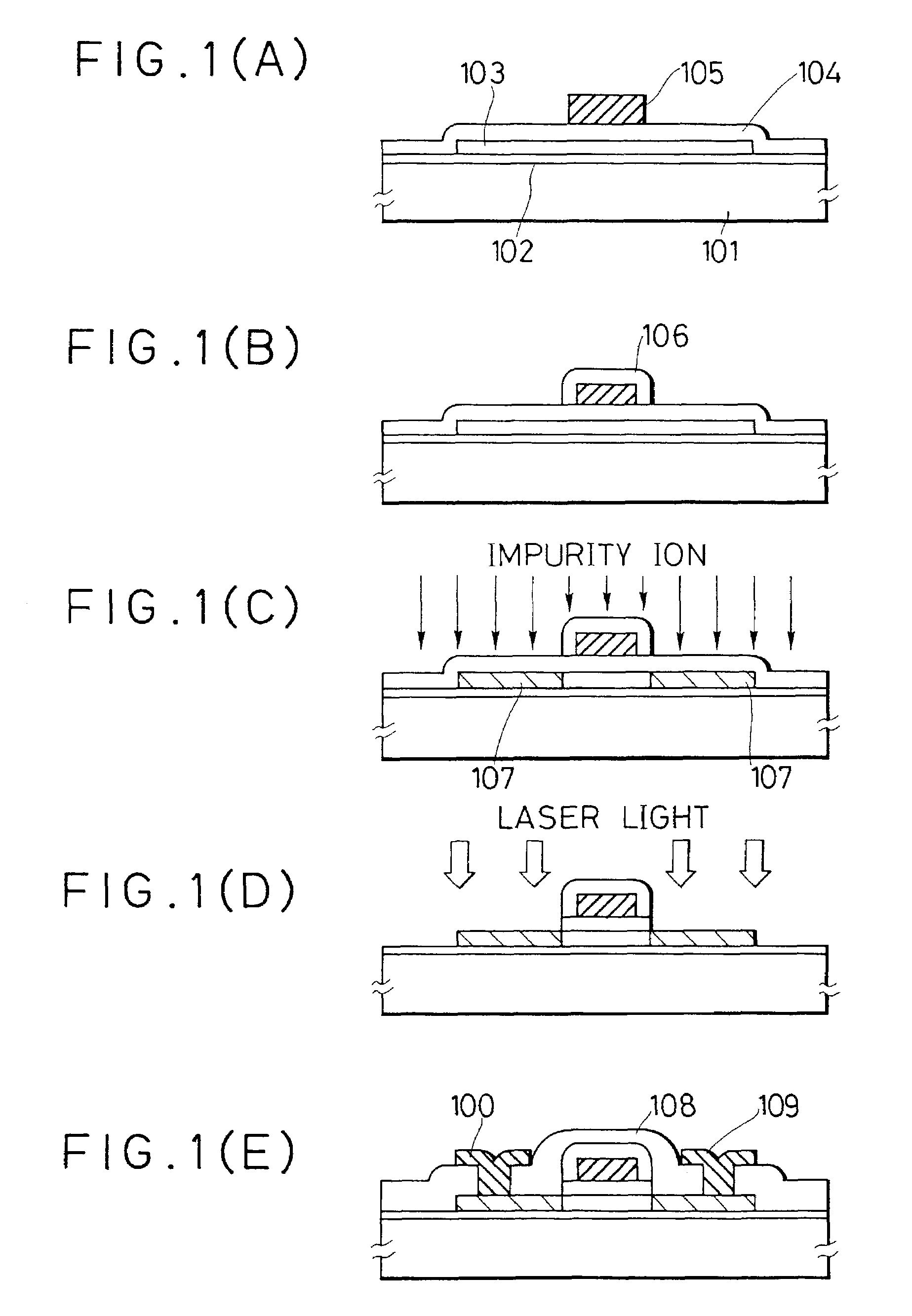
[0028]The present example is illustrated in FIGS. 1(A)-1(E). Silicon oxide was deposited as an insulating base film 102 having a thickness of 1000 Å on a non-alkali glass substrate 101 made of Corning 7059 or the like. A substantially intrinsic amorphous silicon film having a thickness of 1500 Å was formed on the insulating film 102. This amorphous film was annealed at 600° C. for 12 hours to crystallize this film. This crystallized film was photolithographically patterned into island-shaped semiconductor regions 103. A silicon oxide film 104 having a thickness of 1200 Å was deposited as a gate-insulating film. Gate electrodes 105 having a thickness of 6000 Å were fabricated from aluminum (FIG. 1(A)).

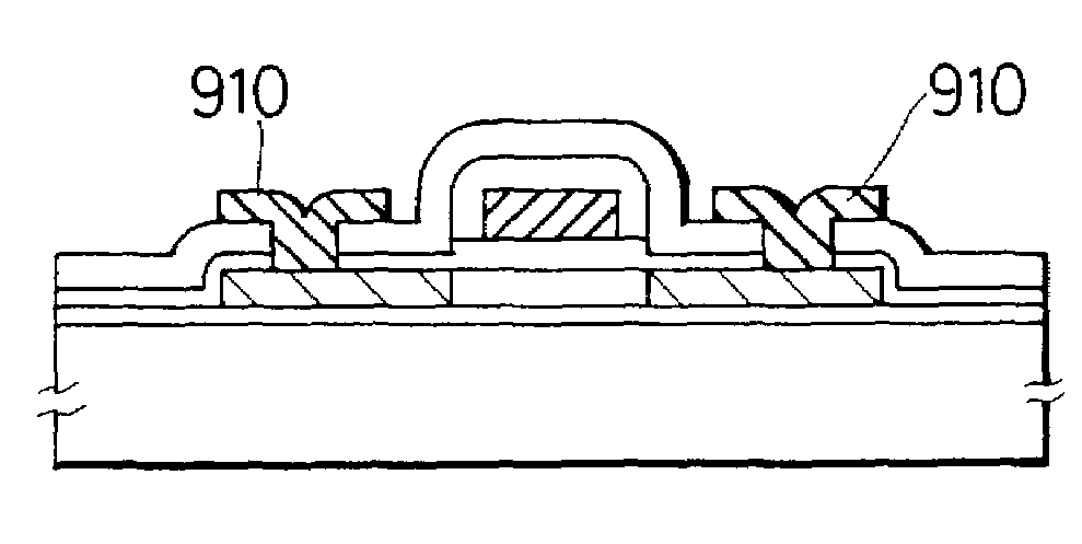
[0029]Then, the gate electrodes were anodized to form an anodic oxide 106 on the top and side surfaces of the gate electrodes and conductive interconnects. The method of fabricating such an anodic oxide and its merits are described in detail in above-cited Japanese Patent application Se...

example 2

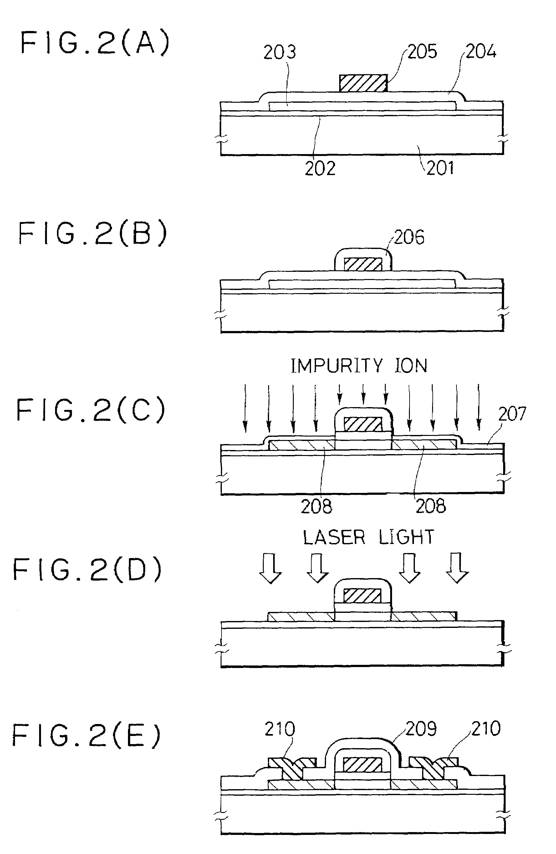
[0034]The present example is illustrated in FIGS. 2(A)-2(E). Silicon oxide was deposited as an insulating base film 202 having a thickness of 1000 Å on a sheet of non-alkali glass 201. A substantially intrinsic amorphous silicon semiconductor film having a thickness of 500 Å was formed on the insulating film 202. The amorphous semiconductor film was illuminated with KrF laser light to crystallize the film. Preferably, the energy density of the laser light was 250 to 400 mJ / cm2. Where the substrate was maintained at 300-550° C. during the laser irradiation, good characteristics were obtained.

[0035]The silicon film crystallized in this way was photolitho-graphically patterned into island-shaped semiconductor regions 203. Silicon oxide was deposited as a gate-insulating film 204 having a thickness of 1200 Å on the island-shaped regions 203. Then, gate electrodes 205 of aluminum having a thickness of 6000 Å were formed (FIG. 2(A)).

[0036]Then, the gate electrodes were anodized to deposit...

example 3

[0041]The present example is illustrated in FIGS. 3(A)-3(D). Silicon oxide was deposited as an insulating base film 302 having a thickness of 1000 Å on a sheet of non-alkali glass 301. A substantially intrinsic amorphous silicon semiconductor film having a thickness of 500 Å was formed on the insulating film 302. The amorphous semiconductor film was illuminated with KrF laser light to crystallize the film. Preferably, the energy density of the laser light was 250 to 400 mJ / cm2. Where the substrate was maintained at 300-550° C. during the laser irradiation, good characteristics were obtained.

[0042]The silicon film crystallized in this way was photolitho-graphically patterned into island-shaped semiconductor regions 303. Silicon oxide was deposited as a gate-insulating film 304 having a thickness of 1200 Å on the island-shaped regions 203. Then, gate electrodes 305 of aluminum having a thickness of 6000 Å were formed.

[0043]Then, the gate electrodes were anodized to deposit an anodic o...


PUM


Abstract

A method of fabricating MIS transistors starts with formation of gate electrode portions. Then, high-speed ions are irradiated through an insulating film to implant impurity ions into a semiconductor region by a self-aligning process, followed by total removal of the insulating film. The laminate is irradiated with laser light or other similar intense light to activate the doped semiconductor region. Another method of fabricating MIS transistors begins with formation of a gate-insulating film and gate electrode portions. Then, the gate-insulating film is removed, using the gate electrode portions as a mask. The semiconductor surface is exposed, or a thin insulating film is formed on this surface. High-speed ions are irradiated to perform a self-aligning ion implantation process. A further method of fabricating MIS transistors starts with formation of a gate-insulating film and gate electrode portions. Then, the gate-insulating film is etched by a self-aligning process, using the gate electrode portions as a mask, to thin the film. Subsequently, high-speed ions are irradiated to form doped regions in a semiconductor region by a self-aligning process.

Description

FIELD OF THE INVENTION[0001]The present invention relates to a method of fabricating MIS transistors and, more particularly, to a method of fabricating MIS transistors having improved crystallinity by illuminating a high-speed ions to implant impurities into a semiconductor region and then improving the crystallinity by laser annealing, lamp annealing, or illumination of other equivalent intense light.BACKGROUND OF THE INVENTION[0002]A structure comprising a semiconductor layer (S) on which a thin insulating film (I) and metal control electrodes (M) are formed is known as a MIS structure. A transistor having such a structure to control the electrical current flowing through the semiconductor layer is referred to as a MIS transistor. Where the insulating film is made of silicon oxide, the transistor is called a MOS transistor.[0003]In the past, the activation step (for removing crystal defects produced on impurity implantation) conducted after the implantation of impurities into such...

Claims


Application Information

Patent Timeline
IPC IPC(8): H01L21/00H01L21/20H01L21/336
CPCH01L21/2026H01L29/66757H01L21/02686H01L21/02422H01L21/02488H01L21/02532H01L21/02675
Inventor YAMAZAKI, SHUNPEI
Owner SEMICON ENERGY LAB CO LTD
Why Eureka
Try Eureka