
Image shifting device, image display, liquid crystal display, and projection image display

a technology of image display and liquid crystal display, which is applied in the direction of color television details, instruments, television systems, etc., can solve the problems of lowering driving power, discharge of charge stored in the corresponding pixel electrode, and lowering contrast ratio, so as to achieve high contrast, increase response speed, and achieve the effect of not increasing driving voltag

Inactive Publication Date: 2007-10-02
SHARP KK
View PDF20 Cites 14 Cited by
  • Summary
  • Abstract
  • Description
  • Claims
  • Application Information

AI Technical Summary

Benefits of technology

The solution effectively suppresses double images and light leakage, achieving high contrast and resolution in liquid crystal display devices, particularly in projection systems, by optimizing the liquid crystal layer's twist angle and spacer placement, and applying appropriate voltages for rapid state switching.

Problems solved by technology

When strong light enters a switching element in an-off state, however, the electric resistance of the switching element is lowered so as to cause a leakage current, and hence, there arises a problem that charge stored in the corresponding pixel electrode is discharged.
Also, a driving voltage at an appropriate level cannot be applied to the pixel electrode and a desired display operation cannot be executed, resulting in causing a problem that a contrast ratio is lowered because light leaks even in a dark state.
In order to attain high refinement by reducing the area occupied by the black matrix, the switching elements and lines are reduced, but when the switching elements and the lines are reduced, the driving power is lowered and the line resistance is increased disadvantageously.
Also, due to restriction of fabrication technology, the switching elements and the lines are difficult to reduce.
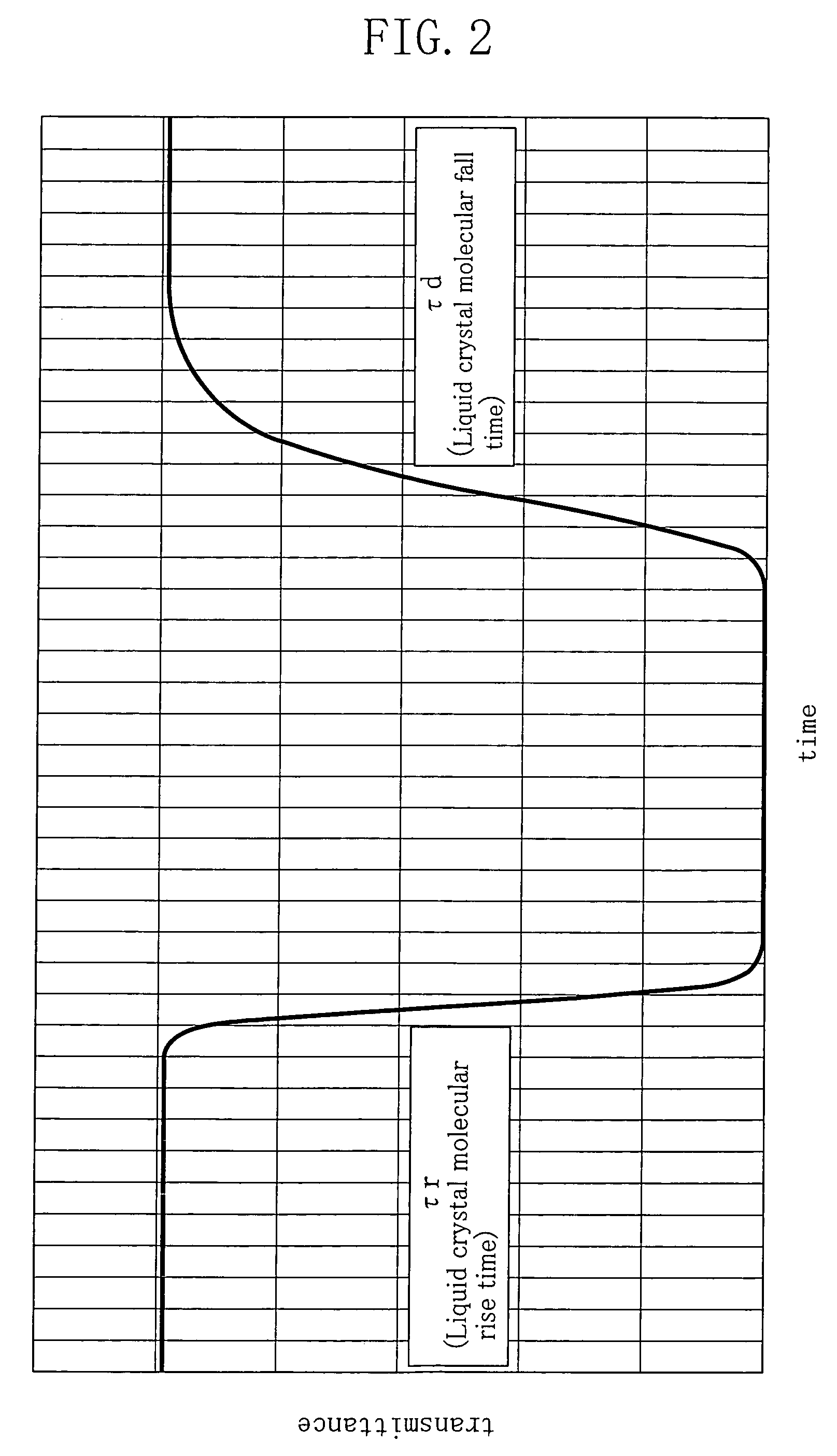
In an actual liquid crystal device, however, it is difficult to rapidly transit the state in response to the voltage application.
When such liquid crystal having the long fall response time τd is used, there arises a problem that polarization cannot be appropriately switched.
However, in a liquid crystal display apparatus, when the concentration of the chiral agent is thus increased, the amplitude of the voltage to be applied through the liquid crystal layer in a voltage on-state should be increased than in a conventional technique, but this is practically difficult in consideration of the performance of a semiconductor thin film transistor working as a switching element in a display region.
Furthermore, there is another problem that as the twist angle peculiar to the liquid crystal is increased, the state of the liquid crystal attained in a voltage off-state is more unstable, and hence, the twist angle of 90° can be kept for merely a short period of time.
Accordingly, the aforementioned technique has not been applied to an actual liquid crystal device.
Moreover, in a liquid crystal display device, when a distance between substrates is varied on a display plane due to deformation of the substrates caused by an external pressure or the like, a threshold voltage is varied, a short-circuit is caused between electrodes of the respective substrates or the orientation of liquid crystal molecules are disturbed, resulting in a problem that good display cannot be produced.
This is because, in the order (a) or (b), when the spacers are formed by using, for example, a photoresist or a photosensitive organic resin, a diluting solvent, a developer and a repellent used in applying such a material may lower the orientation-regulating force of the alignment film, and hence, it is difficult to attain high display quality.
However, since the orientation of the liquid crystal molecules is disturbed in the vicinity of the spacer, light leakage is caused due to an orientation defect region in the vicinity of the spacer, resulting in lowering the contrast ratio.
The lowering of the display quality is particularly serious when the liquid crystal display device is used in a projection image display apparatus.
However, when the mask layer for covering the region where the light leakage is caused is formed, the aperture ratio is lowered, and hence, it is disadvantageously difficult to produce bright display.
Furthermore, the method disclosed in Japanese Laid-Open Patent Publication No. 2001-109005 is difficult to employ for mono domain liquid crystal orientation typically of the TN mode.
This causes light leakage.
Furthermore, a TN liquid crystal display device has a problem that a response speed Doff attained in turning the voltage off is low.
First, when the response speed attained in turning the voltage off is to be improved on the basis of the equation (1), the viscosity η of the liquid crystal is reduced. However, the liquid crystal has physical property values peculiar to the material of the liquid crystal, such as the viscosity, the elastic coefficient, the dielectric constant, the refractive index and the phase transition temperature, and these physical property values are correlated with one another. Therefore, it is difficult to reduce the viscosity alone of the liquid crystal, and hence, this method cannot attain a sufficient effect.
Moreover, when the elastic coefficient K of the liquid crystal is increased, the improvement in the response speed attained in turning the voltage off can be expected, but the elastic coefficient K of the liquid crystal depends upon the chemical structure of the liquid crystal molecule, and hence, it is substantially impossible to set the elastic coefficient K of the liquid crystal independently to a desired value.
In this manner, the improvement in the response speed attained in turning the voltage off on the basis of the equation (1) cannot attain a sufficient effect because of difficulty in improvement of the material with respect to the liquid crystal itself and because of the trade-off relationship between the response speed and the light transmittance with respect to the thickness of the liquid crystal layer.
In this manner, in the method for improving the response speed attained in turning the voltage off by reducing the twist pitch peculiar to the material of liquid crystal, the driving voltage should be increased, and hence, this method is practically difficult to employ in consideration of the performance of a semiconductor transistor or the like working as a switching element.

Method used


Image

  • Image shifting device, image display, liquid crystal display, and projection image display
  • Image shifting device, image display, liquid crystal display, and projection image display
  • Image shifting device, image display, liquid crystal display, and projection image display

Examples


embodiment 1

[0134]First, FIG. 3 is referred. FIG. 3 is a schematic diagram of an image display apparatus according to an embodiment of the present invention.

[0135]The image display apparatus of this embodiment shown in the drawing includes a backlight 1, a liquid crystal display device 2, an image shifting device 3 and an observation optical system 4. The backlight 1 is a light source for illuminating the transmission liquid crystal display apparatus 2, and the liquid crystal display device 2 receives a driving signal and a picture signal from a driving circuit 5 and can display an image with a content corresponding to the picture signal. The observation optical system 4 is an optical system for optically enlarging the image displayed by the liquid crystal display device 2. An observer can observe the image displayed by the liquid crystal display apparatus 2 through the image shifting device 3 and the observation optical system 4.

[0136]Although the transmission liquid crystal display device req...

embodiment 2

[0151]Next, an image display apparatus according to another embodiment will be described with reference to FIG. 6.

[0152]In the image display apparatus of this embodiment, light emitted from a light source 501 (light including at least RGB components) is reflected by a parabolic mirror 502 and changed into substantially parallel beam, and then enters a fly eye lens 503. The fly eye lens 503 is used for uniformly illuminating a liquid crystal panel 504. On the outgoing side of the fly eye lens 503, an aperture 505 for regulating the degree of parallelization of the illumination light entering the liquid crystal panel 504 is provided. The aperture 505 has a rectangular opening and its shape is designed in accordance with the shape of a pixel. The light having passed through the aperture 505 passes through a lens 506 and is separated into RGB light by dichroic mirrors 507R, 507G and 507B. The liquid crystal panel 504 is illuminated by the light having been changed into substantially par...

experiment 1

Method for Experiment

[0232]With respect to a liquid crystal display device having the same structure as that of the above-described embodiment, simulation was carried out for examining the relationship between the twist angle θ (°) peculiar to the material of the nematic liquid crystal and the twist angle φ (°) specified by the alignment film.

[0233]In the simulation, parameters of the liquid crystal were set as follows: the dielectric constant ∈|| along the molecular axis direction of the liquid crystal=14; the dielectric constant ∈ along a direction orthogonal to the molecular axis direction=4; the spread elastic coefficient K11=11 (pN); the twist elastic coefficient K22=6 (pN); the bend elastic coefficient K33=13 (pN); and the anisotropic refractive index Δn=0.15 (at a wavelength of 550 nm). Parameters of the liquid crystal display device were set as follows: the cell gap d of the liquid crystal layer=3 (μm); and the pre-tilt angle=3 (°). The polarizing devices were set so as to s...


PUM

PropertyMeasurementUnit
pre-tilt angleaaaaaaaaaa
voltageaaaaaaaaaa
voltageaaaaaaaaaa

Abstract

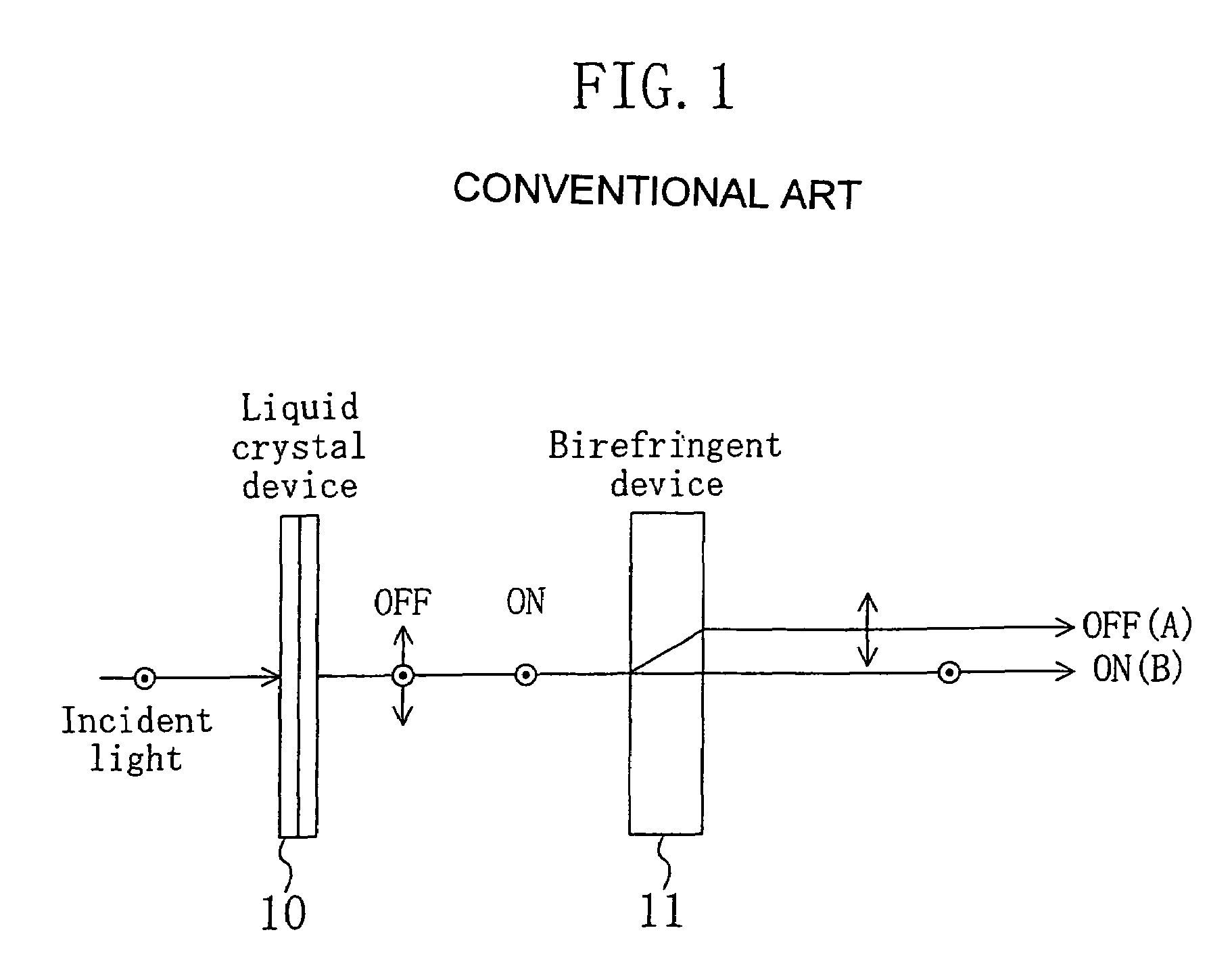
The invention provides an image shifting device including at least one image shifting part for periodically shifting the position of an optical axis. The image shifting part includes a liquid crystal device 10 for switching a polarization direction of light between two orthogonal directions in accordance with High / Low level of an applied voltage, and a birefringent device 11 having different refractive indexes depending upon the polarization direction of the light. The liquid crystal device 10 and the birefringent device 11 are disposed to transmit light in this order. A liquid crystal layer included in the liquid crystal device 10 is made of a TN liquid crystal layer that satisfies a relationship formula of 0.25<d / p<1, wherein a natural pitch length is indicated by p and a cell gap is indicated by d, and is disposed to be twisted at 90° within the liquid crystal cell.

Description

CROSS REFERENCE TO RELATED APPLICATIONS[0001]This application is a Section 371 of International Patent Application No. PCT / JP02 / 12462, filed Nov. 28, 2002, the disclosure of which is incorporated herein by reference.TECHNICAL FIELD[0002]The present invention relates to an image shifting device, and, more specifically, to an image shifting device suitable for use in a head mount display (hereinafter referred to as the “HMD”) or a projection image display apparatus (projector), and an image display apparatus including the image shifting device.[0003]Furthermore, the present invention relates to a liquid crystal display device and a projection image display apparatus including the liquid crystal display device, and, in some embodiments it relates to a liquid crystal display device having a spacer provided between a pair of substrates and a projection image display apparatus including the liquid crystal display device.[0004]Moreover, an embodiment of the present invention relates to a t...

Claims


Application Information

Patent Timeline
Patent Type & Authority Patents(United States)
IPC IPC(8): G02F1/1335G02F1/1333H04N5/74H04N9/31
CPCH04N9/3197H04N9/3108H04N5/7441
Inventor KURIHARA, TAKASHIKUME, YASUHIRONAKANISHI, HIROSHITAMAI, KAZUHIKO
Owner SHARP KK
Learn More