Plasma dielectric etch process including ex-situ backside polymer removal for low-dielectric constant material
- Summary
- Abstract
- Description
- Claims
- Application Information
AI Technical Summary
Benefits of technology
Problems solved by technology
Method used
Image
Examples
Embodiment Construction
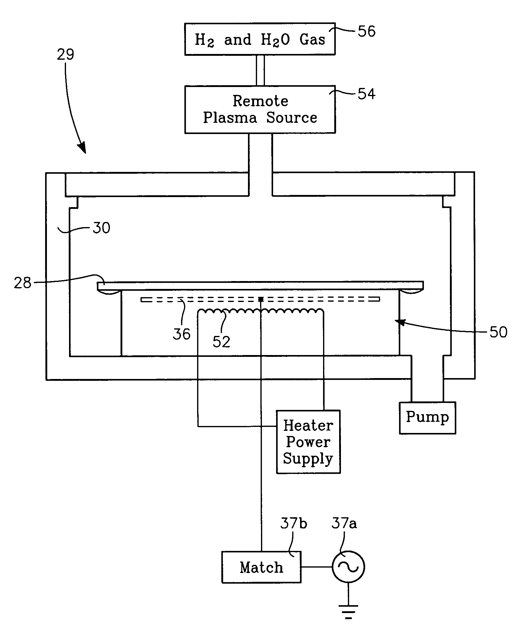
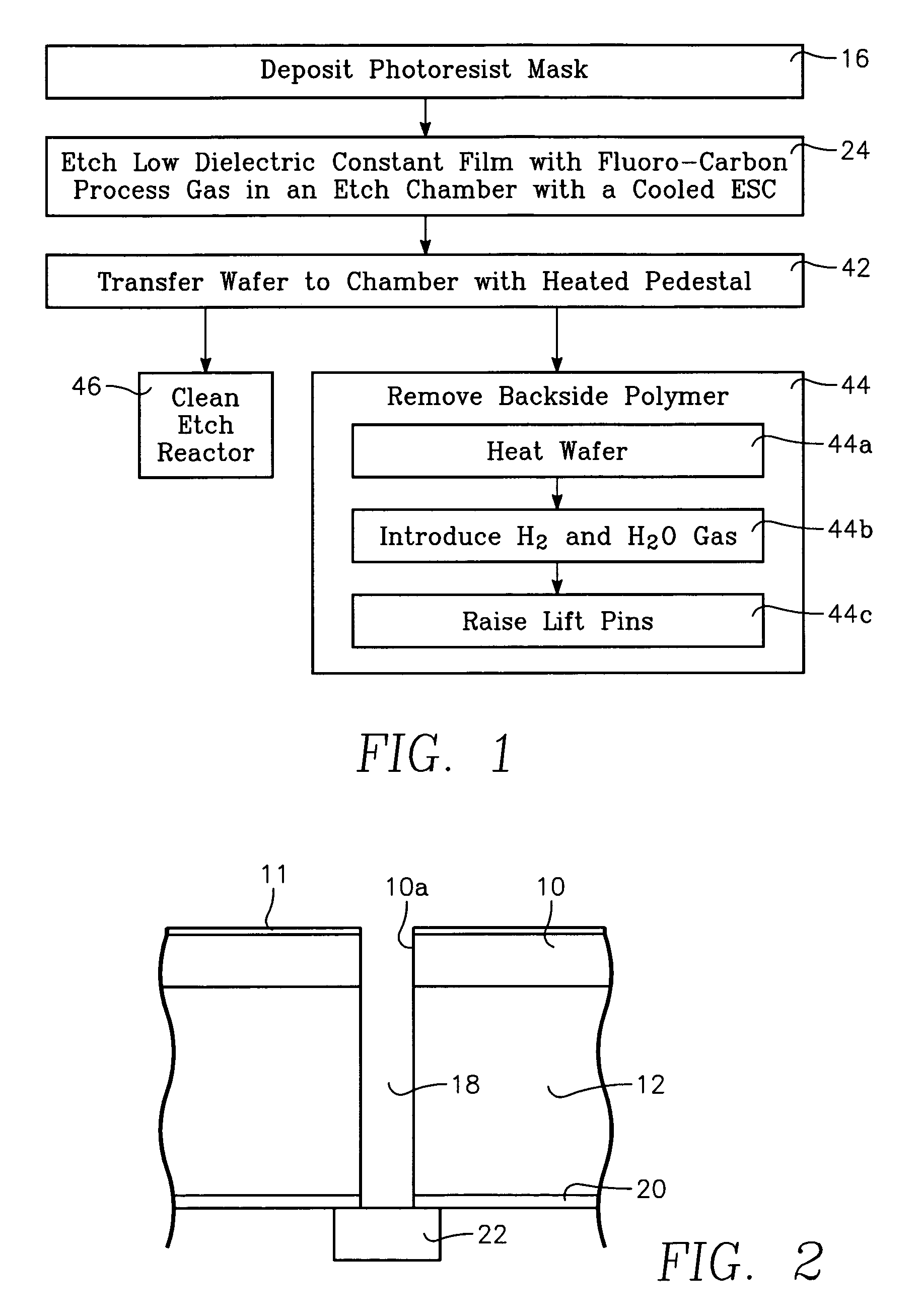
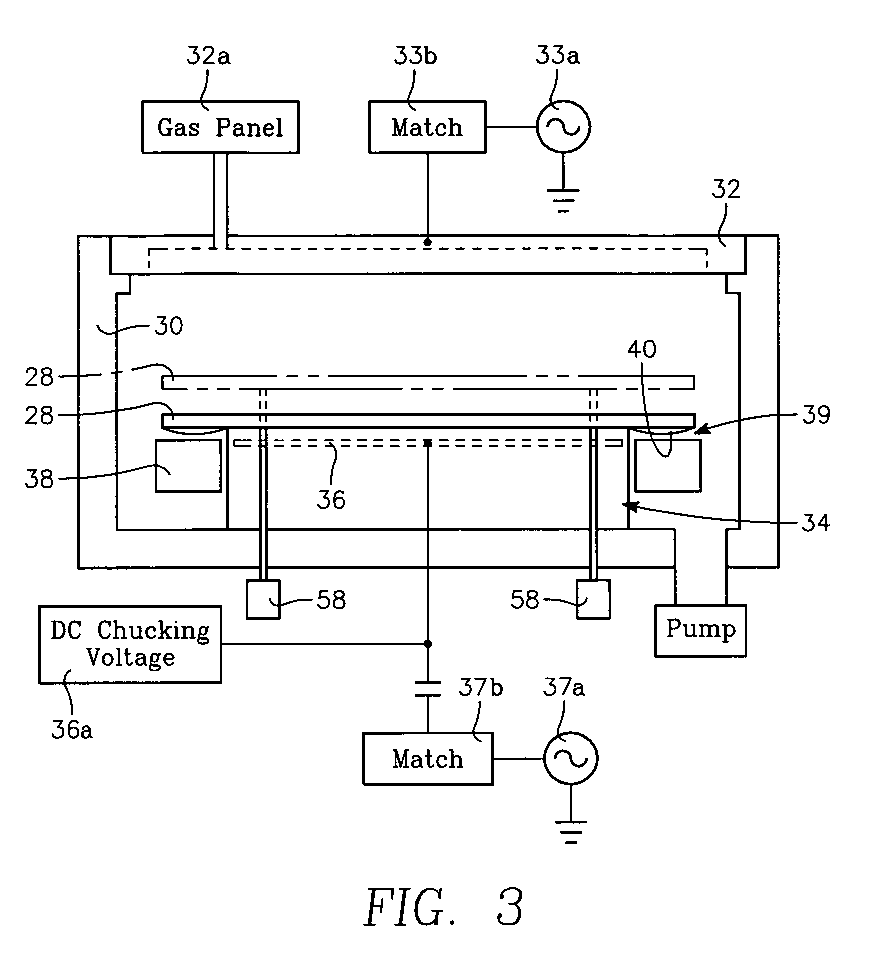
[0011]The invention is based upon our discovery of an etch process for a low dielectric constant material including a post etch polymer removal step that thoroughly removes both backside polymer and photoresist with no appreciable damage to the low dielectric constant insulator layer (e.g., porous carbon-doped silicon dioxide or a porous organo-silicate material), and does so in less than 60 seconds. An etch process embodying the invention is depicted in FIG. 1, while FIG. 2 depicts one example of a thin film structure that can be formed using the process of FIG. 1. A photoresist mask 10 depicted in FIG. 2 is deposited on a dielectric layer 12, the mask 10 having an aperture 10a corresponding to a feature 18 that is to be etched in the dielectric layer 12. This corresponds to the step of block 16 of FIG. 1. The feature may be a narrow via 18. The via 18 extends through the dielectric layer 12 and through a barrier layer 20 to expose the top surface of a copper line 22. The dielectri...
PUM
| Property | Measurement | Unit |
|---|---|---|
| Diameter | aaaaa | aaaaa |
| Dielectric constant | aaaaa | aaaaa |
Abstract
Description
Claims
Application Information
 - R&D
- Intellectual Property
- Life Sciences
- Materials
- Tech Scout
- Unparalleled Data Quality
- Higher Quality Content
- 60% Fewer Hallucinations
Browse by: Latest US Patents, China's latest patents, Technical Efficacy Thesaurus, Application Domain, Technology Topic, Popular Technical Reports.
© 2025 PatSnap. All rights reserved.Legal|Privacy policy|Modern Slavery Act Transparency Statement|Sitemap|About US| Contact US: help@patsnap.com


