Composition for forming a porous film prepared by hydrolysis and condensation of an alkoxysilane using a trialkylmethylammonium hydroxide catalyst
- Summary
- Abstract
- Description
- Claims
- Application Information
AI Technical Summary
Benefits of technology
Problems solved by technology
Method used
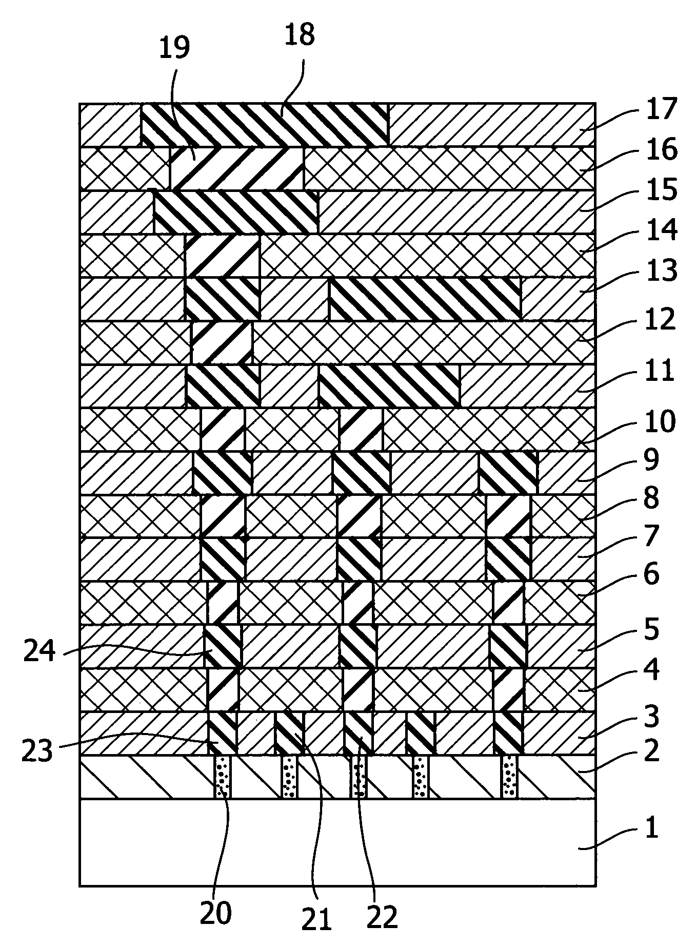
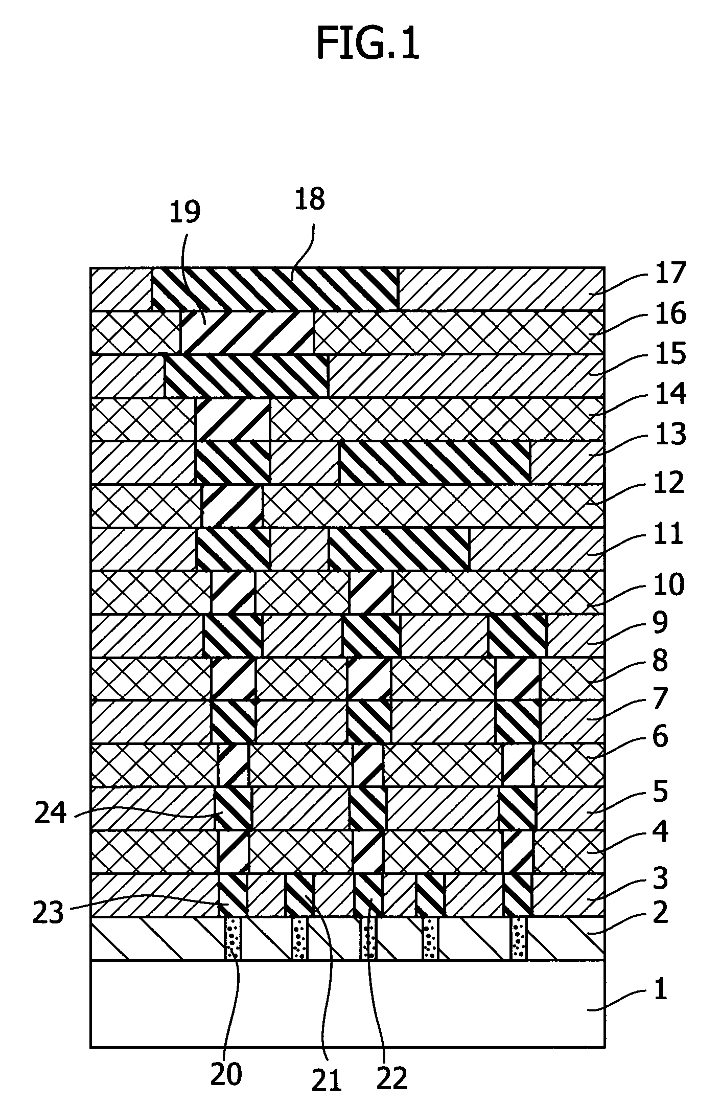
Image

Examples
example 1
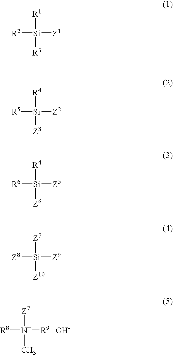
[0059]The 21.5 g of an aqueous 20 wt % solution of tetramethylammonium hydroxide (made by Tama Chemical Company) was added to a mixture of 237 g of ultra-pure water and 471 g of ethanol and then uniformly stirred. The mixture of 44.9 g of methytrimethoxysilane and 68.6 g of tetraethoxysilane was added dropwise thereto. The resulting mixture was reacted at 60° C. for two hours, then the pH thereof was adjusted to be 4.3 by adding an aqueous solution of maleic acid. Propylene glycol monopropyl ether was added thereto, and concentrated at a reduced pressure until the siloxane concentration became 10 wt %. The resulting solution was then filtered with a filter made of Teflon™ having pore diameter of 0.05 μm, and consequently, coating composition (1) was obtained. The weight-average molecular weight of the product obtained by the hydrolysis and condensation of the alkoxysilane was about 100,000 as the result of measurement by GPC.
example 2
[0060]Coating composition (2) was obtained in the same manner as Example 1 except that 6.3 g of triethylmethylammonium hydroxide was used in the place of the 21.5 g of an aqueous 20 wt % solution of tetramethylammonium hydroxide. The triethylmethylammonium hydroxide had been produced by the reaction between triethylamine and dimethyl carbonate. The weight-average molecular weight of the product obtained by the hydrolysis and condensation of the alkoxysilane was about 120,000 as the result of measurement by GPC.
PUM
| Property | Measurement | Unit |
|---|---|---|
| Fraction | aaaaa | aaaaa |
| Fraction | aaaaa | aaaaa |
| Composition | aaaaa | aaaaa |
Abstract
Description
Claims
Application Information
 - R&D
- Intellectual Property
- Life Sciences
- Materials
- Tech Scout
- Unparalleled Data Quality
- Higher Quality Content
- 60% Fewer Hallucinations
Browse by: Latest US Patents, China's latest patents, Technical Efficacy Thesaurus, Application Domain, Technology Topic, Popular Technical Reports.
© 2025 PatSnap. All rights reserved.Legal|Privacy policy|Modern Slavery Act Transparency Statement|Sitemap|About US| Contact US: help@patsnap.com