Method and apparatus for producing rectangular contact holes utilizing side lobe formation
a technology of side lobes and contact holes, applied in the direction of photomechanical devices, instruments, photo-taking processes, etc., can solve problems such as constructive interference of diffraction patterns
- Summary
- Abstract
- Description
- Claims
- Application Information
AI Technical Summary
Problems solved by technology
Method used
Image

Examples
example 1
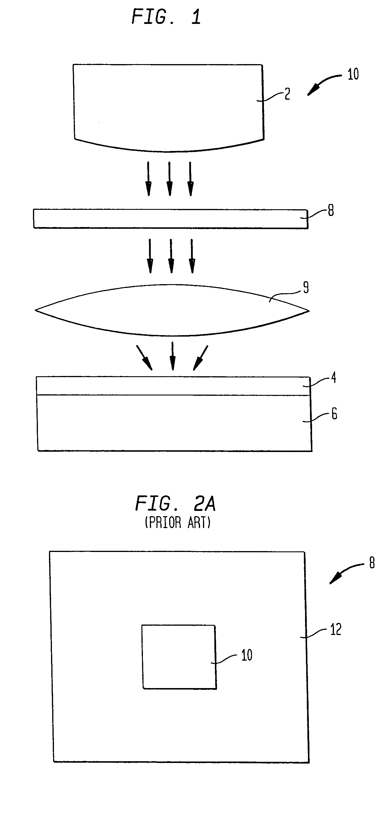
[0021]FIG. 3a illustrates a first exemplary photomask 8 used to create a pattern of small quadratic contact holes 18. Photomask 8 comprises attenuating region 12 and open windows 10. The resulting pattern on photoresist layer 4 is shown in FIG. 3b. The desired pattern to be exposed on photoresist layer 4 is an array of square shaped contact holes of size 225 nm by 225 nm. Photoresist layer 4 was comprised of a 5000 Angstrom thick layer of JSR M22G photoresist available from JSR, Corp., Tokyo, Japan, with a bottom antireflective coating of approximately 900 Angstroms thickness. The wafer was exposed using a Nikon DUV Scanner S203B with a numerical aperture of 0.68.
[0022]The photomask itself was formulated using attenuated phase shift photomask technology wherein attenuating region 12 provided for 6% transmittance. The pattern on the photomask was 4× the desired pattern on layer 4, with appropriate demagnification being accomplished via focusing lens 9. Deep UV light source 2 provides...
example 2
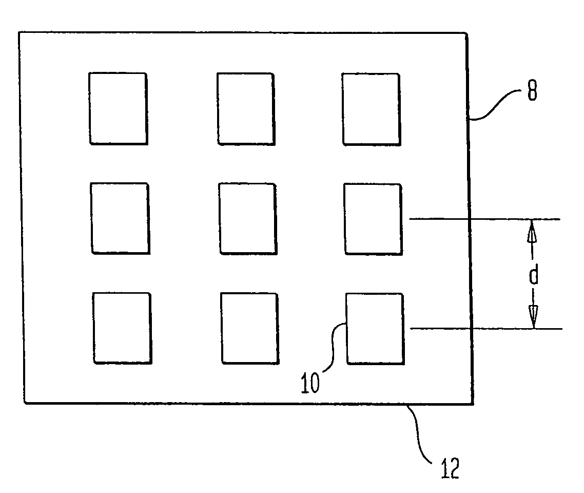
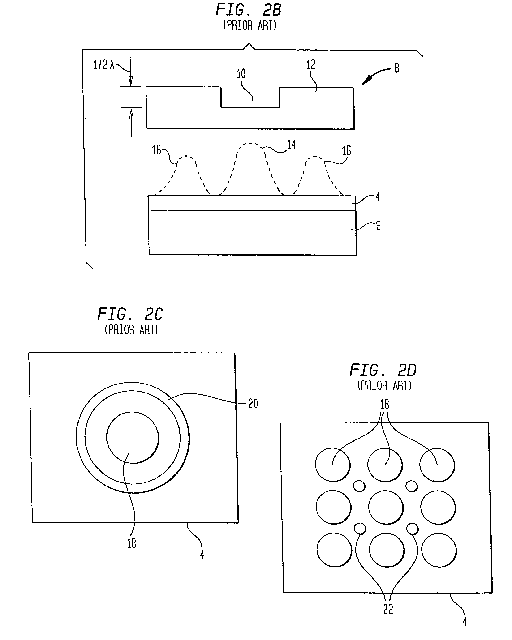
[0026]In this example, photoresist layer 4 has been exposed using the methods of any of the preceding examples, resulting in the pattern illustrated in FIG. 3b. Only the center-most contact hole 18, however, is needed for the circuit, the surrounding contact holes having been formed solely to ensure that the center-most contact hole has an acceptable square shape and to prevent undesirable side lobe features for forming around the desired contact hole.
[0027]In order to block out (remove) the unnecessary contact holes, a second exposure involving a second photoresist layer and a blocking photomask is employed. This blocking photomask will have an open window 10 only corresponding to the desired (center-most) contact hole, and the remaining contact holes will be placed under an attenuating region 12 of the blocking photomask. In this way, only the desired contact hole will be exposed during the second exposure step. In order to prevent the first photoresist layer 4 from being dissolve...
example 3
[0028]In this example. photoresist layer 4 has been exposed using the methods of the preceding examples, resulting in the pattern illustrated in FIG. 3b. FIGS. 4a through 4g illustrate the process steps to eliminate the unnecessary contact holes. FIG. 4aprovides a cross section view of semiconductor wafer 6, including conducting region 24 formed atop the wafer and insulating layer 26 formed atop the conducting region. Photoresist layer 4 has been photolithographically processed as described above, resulting in the patterned layer 4 illustrated in FIG. 4a. As will be apparent to one skilled in the art, desired contact bole 10′ is intended to provide a conductive pathway through insulating layer 26 by which electrical contact with buried conductive region 24 can be made. The conductive pathway through insulating layer 26 is formed by filling contact hole 10′ with conductive material.
[0029]In FIG. 4b, insulating layer 26, which is preferably a silicon dioxide or polysilicon layer is et...
PUM
| Property | Measurement | Unit |
|---|---|---|
| light wavelength | aaaaa | aaaaa |
| wavelength | aaaaa | aaaaa |
| wavelength | aaaaa | aaaaa |
Abstract
Description
Claims
Application Information
 - R&D
- Intellectual Property
- Life Sciences
- Materials
- Tech Scout
- Unparalleled Data Quality
- Higher Quality Content
- 60% Fewer Hallucinations
Browse by: Latest US Patents, China's latest patents, Technical Efficacy Thesaurus, Application Domain, Technology Topic, Popular Technical Reports.
© 2025 PatSnap. All rights reserved.Legal|Privacy policy|Modern Slavery Act Transparency Statement|Sitemap|About US| Contact US: help@patsnap.com