
Word line driver circuits for use in semiconductor memory and driving method thereof

a technology of word line driver and semiconductor memory, which is applied in the direction of information storage, static storage, digital storage, etc., can solve the problems of memory cells connected to non-selected word lines like wlb>1/b>, data interference by floating voltage, and chip size and current consumption. , to achieve the effect of reducing chip size and current consumption, high integration and low power consumption

Inactive Publication Date: 2007-05-22
SAMSUNG ELECTRONICS CO LTD
View PDF5 Cites 28 Cited by
  • Summary
  • Abstract
  • Description
  • Claims
  • Application Information

AI Technical Summary

Benefits of technology

This patent describes a word line driver circuit and method for a semiconductor memory device. The circuit boosts only the selected word line, reducing chip size and power consumption. It prevents the non-selected word line from being affected, ensuring stable operation. The circuit includes a capacitor that boosts the output node to a higher voltage level than the power source voltage during the selected operating mode. The circuit also includes transistors to control the output and control the capacitor. The driving method involves transferring the output signal of the word line decoding circuit to the control node, floating the output node and control node, and increasing the output node to a higher voltage level than the power source voltage using the capacitor. The technical effects of this invention include reducing power consumption, improving integration, and stabilizing operation.

Problems solved by technology

Thus the chip size becomes larger and the power consumption increases.
This has a disadvantage that the data of memory cells connected to non-selected word lines like WL1 may be interfered with by a floating voltage because the non-selected word lines attain a floating state.
In other words, the voltage level difference of word line WL0 is insufficient for the operation, and in the worst case, there may be the case that a word line cannot be boosted.

Method used


Image

  • Word line driver circuits for use in semiconductor memory and driving method thereof
  • Word line driver circuits for use in semiconductor memory and driving method thereof
  • Word line driver circuits for use in semiconductor memory and driving method thereof

Examples


Embodiment Construction

[0027]Exemplary embodiments of the present invention will be described with reference to FIGS. 3 and 6.

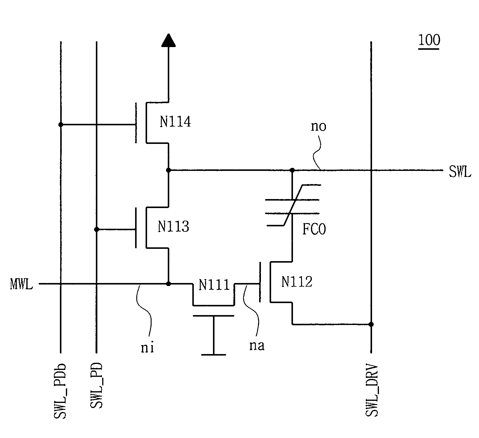
[0028]FIG. 3 illustrates a word line driver circuit for use in a semiconductor memory device according to an exemplary embodiment of the present invention. The word line driver circuit according to an exemplary embodiment drives word lines SWL individually connected with the memory cells that constitute a memory cell array of a semiconductor memory device.

[0029]A non-selected operating mode described shortly indicates an operating mode of a word line driver circuit for the case where a word line is not selected in a read or write operation. A selected operating mode indicates an operating mode of a word line driver in the case where a word line is selected and the output signal of a word line decoding circuit (not shown) is asserted. A stand-by mode denotes an operating mode of a word line driver where a read or write operation is not to be performed and a word line is not selected...


PUM


Abstract

Disclosed is a word line driver circuit and a driving method thereof. An input to the circuit has a ground voltage level during a non-selected operating mode and, as the output signal of a word line decoding circuit, is applied at a power source voltage level during a selected operating mode. The output of the circuit has a ground voltage level during the non-selected operating mode and applies a higher voltage than the power source voltage to a word line connected to a memory cell during the selected operating mode. Optionally, a capacitor boosts the output voltage during the selected operating mode.

Description

CROSS-REFERENCE TO RELATED FOREIGN APPLICATION[0001]This application claims the priority of Korean Patent Application No. 10-2004-0045298, filed on Jun. 18, 2004, in the Korean Intellectual Property Office, the disclosure of which is incorporated herein in its entirety by reference.BACKGROUND OF THE INVENTION[0002]1. Field of the Invention[0003]The present invention relates to an integrated circuit memory device, and more particularly, to a word line driver circuit for supplying a voltage that is higher than the power source voltage requiring an internal boost voltage, and a driving method thereof.[0004]2. Description of the Related Art[0005]In a typical semiconductor memory device that operates at a low voltage, a bootstrap circuit is used to apply a higher voltage than the operating voltage to the capacitor of a memory cell in order to increase the operating speed in reading or writing data. In other words, to prevent or substantially reduce errors in read or write operations, the...

Claims


Application Information

Patent Timeline
Patent Type & Authority Patents(United States)
IPC IPC(8): G11C8/00G11C5/14G11C8/08G11C11/22
CPCG11C8/08G11C11/22G11C5/14
Inventor JEON, BYUNG-GIL
Owner SAMSUNG ELECTRONICS CO LTD
Learn More