Antenna and communication device
a communication device and antenna technology, applied in the field of new antennas, can solve the problems of inability to maintain the efficiency over plural bands, inability to reduce the size of the antenna portion, and inability to reduce the size of the module, so as to improve the conversion efficiency of electromagnetic waves, facilitate handling, and improve the effect of manufacturing efficiency
- Summary
- Abstract
- Description
- Claims
- Application Information
AI Technical Summary
Benefits of technology
Problems solved by technology
Method used
Image

Examples
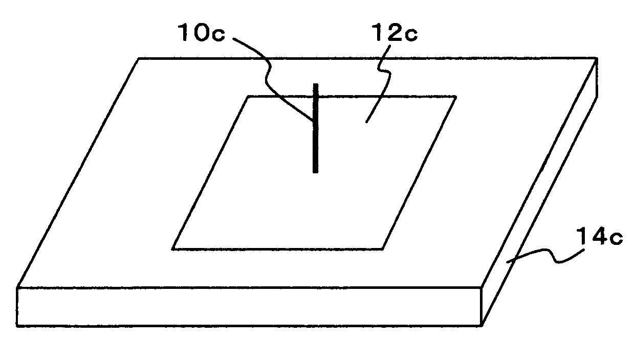
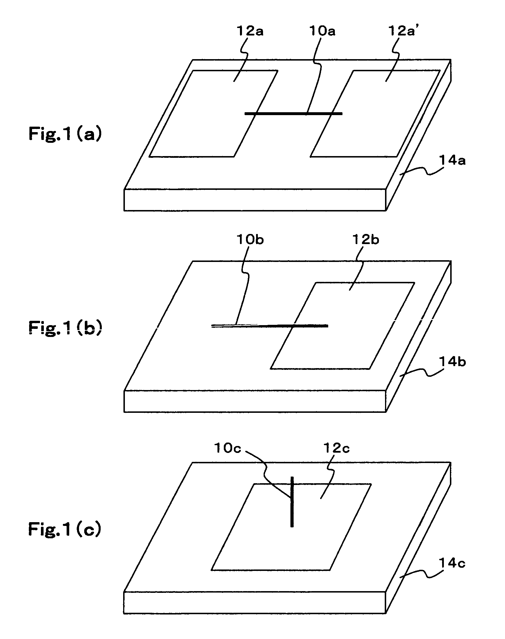
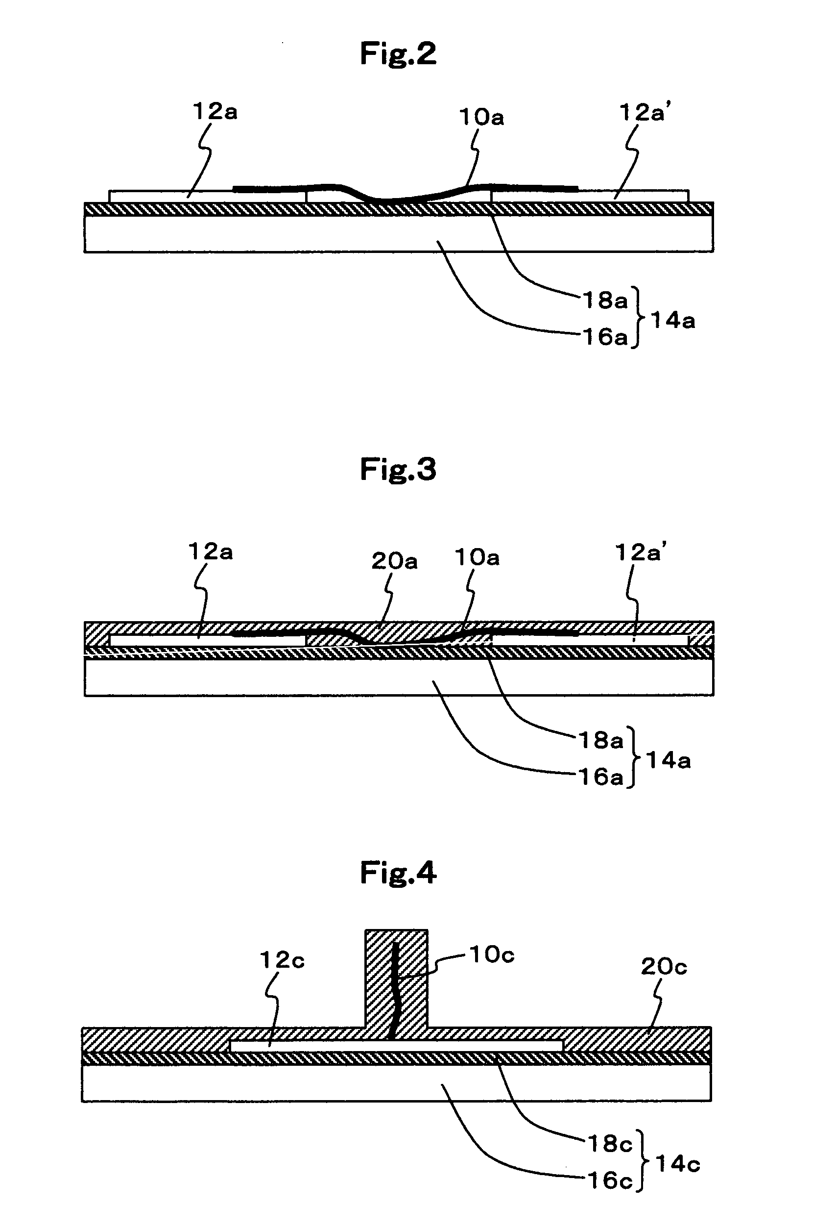
first example
(Fabrication of Antenna)
[0109]First, a pair of electrodes for connecting a multi-wall carbon nanotube were formed on an SiO2 layer side surface of an SiO2 / Si substrate (the thickness of an Si substrate as a support plate was 500 μm, and the thickness of an SiO2 layer as a dielectric layer was 500 nm) so as to adjust a gap between those two electrodes to 2.5 μm. A mask deposition method was used as the forming method, and an electrode material as used was Au / Cr. The thickness of the electrodes was set to 50 nm.
[0110]One multi-wall carbon nanotube (40 nm in diameter and 4 μm in length) fabricated through the in-magnetic-field arc electric discharge process was so arranged as to bridge the gap between the pair of electrodes thus obtained, and fixed. More specifically, a micromanipulator was introduced in an scanning electron microscope (SEM). The detailed procedure will be described below.
[0111]First, a cathode deposit containing a high-purity multi-wall carbon nanotube that had been c...
second example
(Fabrication of Antenna)
[0116]A pair of Au / Cr electrodes were fabricated on an SiO2 layer side surface of the SiO2 / Si substrate with a gap of 10 μm therebetween as in the first example. The thickness of the electrodes was 50 nm.
[0117]The single-wall carbon nanotube composed through the arc electric discharge method was purified (about 1 nm in the mean diameter), and dispersed in dimethylformamide at the ratio of 10 g / 1. One droplet of the single-wall carbon nanotube was dropped in the gap between the pair of electrodes by using a micropipette and was then naturally dried.
[0118]The antenna of this example was fabricated in the above-manner. FIG. 11 is an SEM photographic image (magnification of 3000 times) obtained by extracting only a portion at which a carbon nanotube is located and enlarging the extracted portion in the antenna in accordance with this example of the present invention. In FIG. 11, the single-wall carbon nanotubes seem to be white thin lines, and it is found that pl...
PUM
 Abstract
Description
Claims
Application Information
 - R&D
- Intellectual Property
- Life Sciences
- Materials
- Tech Scout
- Unparalleled Data Quality
- Higher Quality Content
- 60% Fewer Hallucinations
Browse by: Latest US Patents, China's latest patents, Technical Efficacy Thesaurus, Application Domain, Technology Topic, Popular Technical Reports.
© 2025 PatSnap. All rights reserved.Legal|Privacy policy|Modern Slavery Act Transparency Statement|Sitemap|About US| Contact US: help@patsnap.com