Liquid crystal display device

A liquid crystal display device, liquid crystal technology, applied in nonlinear optics, instruments, optics, etc., can solve the problems of lower transmittance, achieve the effect of increasing transmittance, reducing directivity, and preventing mixed colors

Inactive Publication Date: 2009-04-29
HITACHI DISPLAYS
View PDF6 Cites 14 Cited by
  • Summary
  • Abstract
  • Description
  • Claims
  • Application Information

AI Technical Summary

Problems solved by technology

Also in this IPS method there is a capacitive line for forming a capacitor, so the transmittance is reduced

Method used


Image

  • Liquid crystal display device
  • Liquid crystal display device
  • Liquid crystal display device

Examples


Embodiment 1

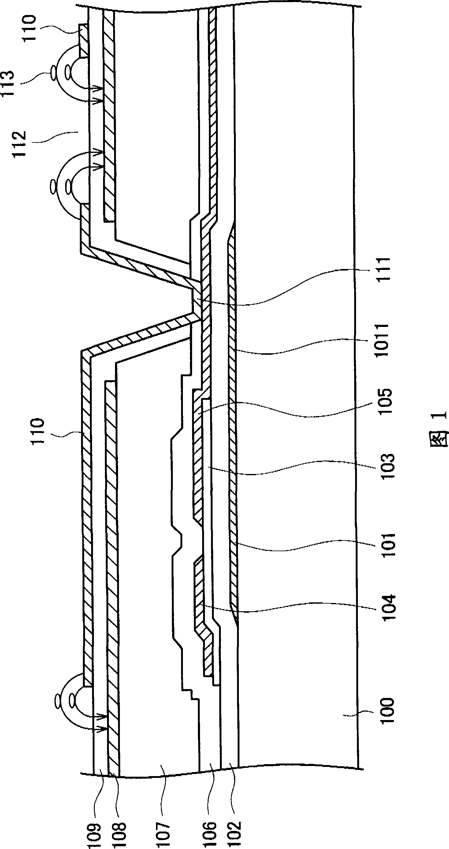
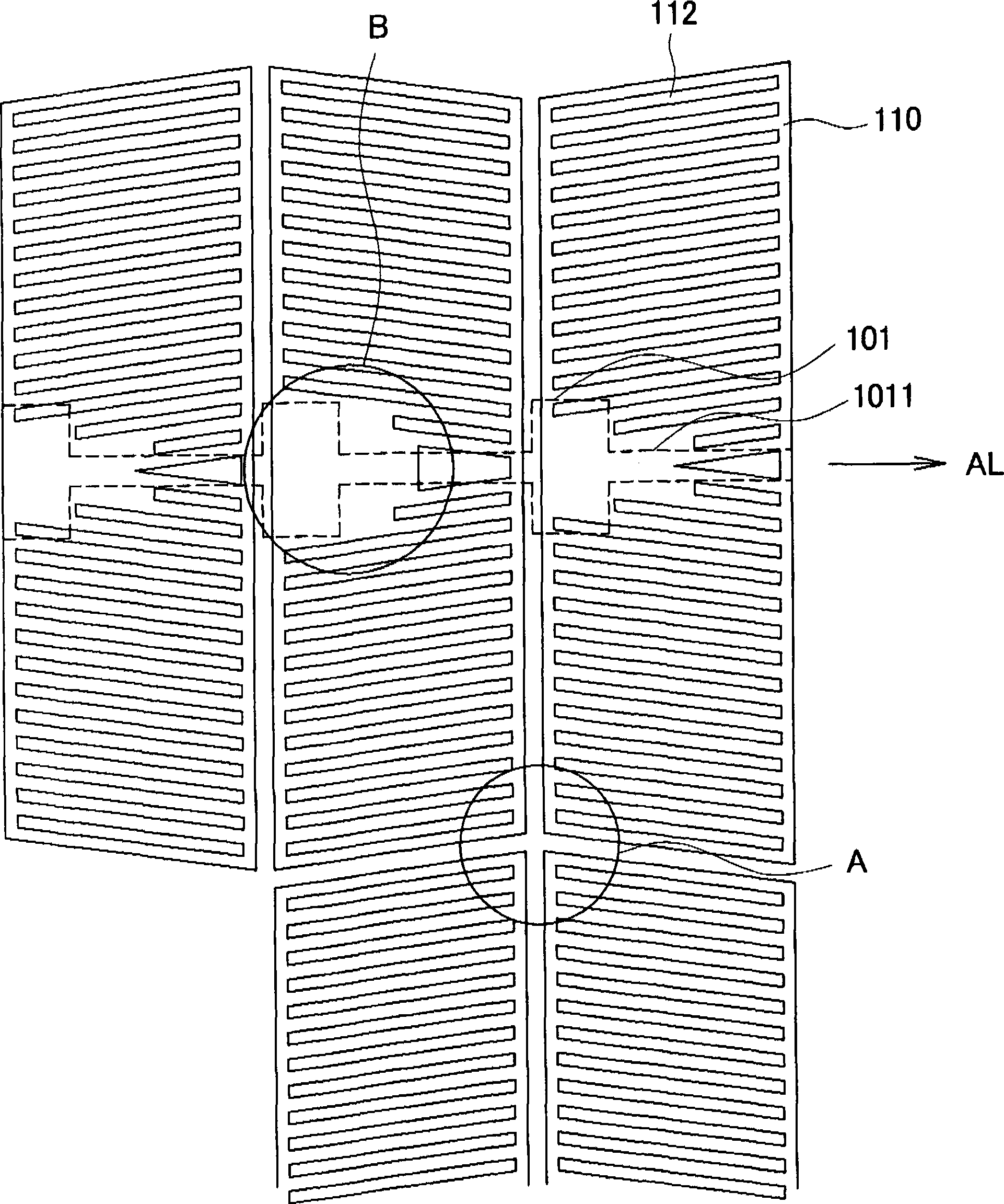
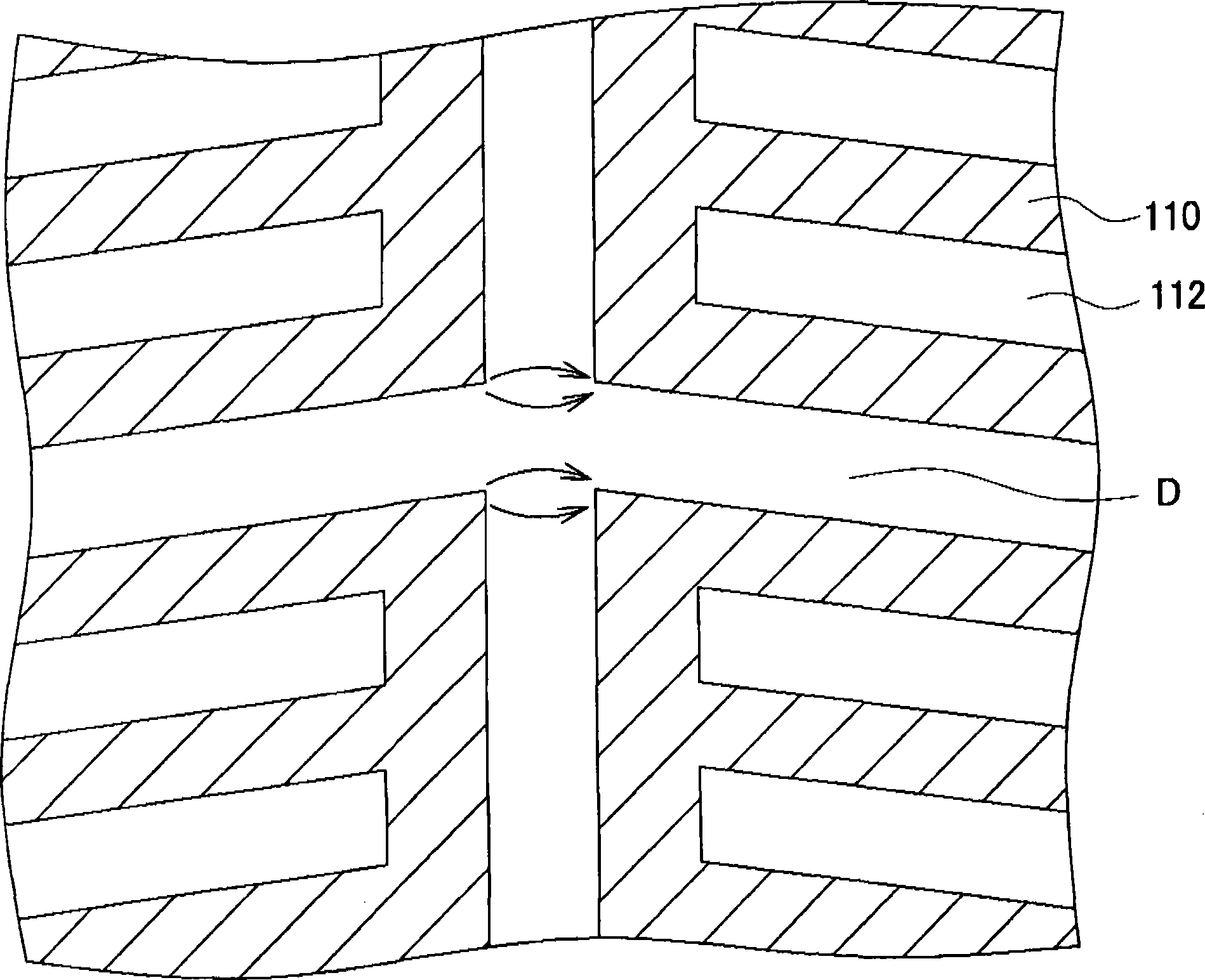
[0060] figure 2 It is a plan view showing the arrangement of pixels in the TFT substrate 100 of Example 1. image 3 Yes means figure 2 An enlarged plan view of part A of the boundary of the pixel shown. Figure 4 Yes means figure 2 An enlarged perspective view of part B near the TFT.

[0061] in figure 2 In order to simplify the drawing, only the pixel electrode 110 and the scan line 1011 are described. in figure 2 In the middle, the pixel is a horizontal trapezoid. In the past, the pixel was defined by the area surrounded by the image signal line and the scan line, but in this embodiment, the pixel is defined by the pixel electrode 110 itself. In the vertical direction, the pixels are arranged in a horizontal trapezoid that alternately changes directions (reverses them), forming a dense structure.

[0062] Also, in this embodiment, in the horizontal direction, the pixels are arranged in a horizontal trapezoid to alternately change directions (reverse them).

[0063] In addi...

Embodiment 2

[0088] In the present invention, in order to increase the transmittance as much as possible, the overlapping area of ​​the scan line 1011 (the gate electrode 101) and the drain electrode 105 is increased. In this case, the capacitance Cgd between the gate electrode 101 and the drain electrode 105 becomes larger. When the capacitance Cgd increases, the so-called voltage displacement of the pixel electrode 110 changes due to the change in the gate voltage. Therefore, the capacitance Cgd is preferably smaller. This embodiment provides a structure to reduce the capacitance Cgd.

[0089] The pixel position in this embodiment is the same as figure 2 the same. figure 2 The structure of the part B shown is different from the structure of the part B of the first embodiment. Figure 6 It is a plan view showing a configuration example in which the capacitance Cgd between the scanning line 1011 (gate electrode 101) and the drain electrode 105 is reduced in this embodiment. in Figure 6 In t...


PUM


Abstract

The present invention realizes an IPS liquid crystal display device which exhibits small directivity of viewing angle and high brightness. Below a pixel electrode having a comb-teeth-shaped electrode and having a laterally-extending trapezoidal profile, a planar common electrode not shown in the drawing is formed by way of an insulation film. When a video signal is applied to the pixel electrode, an electric field is generated between the pixel electrode and the common electrode via slit portions formed in the pixel electrode thus controlling liquid crystal molecules. The pixel electrodes are arranged in a packed state by alternately reversing the direction of the trapezoidal shape in the longitudinal direction. Since a light blocking film is not present between two pixel electrodes arranged adjacent to each other in the longitudinal direction, the liquid crystal display device can acquire high transmissivity. As a result, a liquid crystal display device having high brightness can be realized.

Description

Technical field [0001] The present invention relates to a liquid crystal display device, and more particularly, to a liquid crystal display device of a lateral electric field method with excellent viewing angle characteristics and brightness characteristics. Background technique [0002] In a liquid crystal display device, a TFT substrate on which pixel electrodes, thin film transistors (TFT), etc. are formed in a matrix, and a counter substrate on which a color filter or the like is formed at a position corresponding to the pixel electrode facing the TFT substrate. Liquid crystal is sandwiched between the TFT substrate and the counter substrate. And, the liquid crystal molecules are driven and the transmittance of light is controlled for each pixel, thereby forming an image. [0003] There is a problem of viewing angle characteristics in liquid crystal display devices. The viewing angle characteristic is a phenomenon in which brightness changes and chromaticity changes when the ...

Claims


Application Information

Patent Timeline
Patent Type & Authority Applications(China)
IPC IPC(8): G02F1/1362G02F1/1343G02F1/1337G02F1/1339
CPCG02F2201/40G02F1/134363
Inventor 丹野淳二森本政辉佐佐木亨
Owner HITACHI DISPLAYS
Why Eureka
Try Eureka