Optical information medium and production method therefor
a technology of optical information and production method, applied in the field of optical information media, can solve the problems of insufficient scratch/abrasion resistance and sufficient anti-staining property against organic stains, errors in recording/reproducing optical information, and limited highest achievable abrasion resistance, so as to reduce the friction coefficient of the surface, suppress the generation of scratches, and improve the scratch resistance of the surface
- Summary
- Abstract
- Description
- Claims
- Application Information
AI Technical Summary
Benefits of technology
Problems solved by technology
Method used
Image
Examples
examples
[0080]The present invention will now be described in detail with reference to examples, which are not intended to limit the scope of the invention in any way.
[Preparation of Compositions for Hard Coat Layer]
[0081]The following base compositions (a), (b), and (c) for ultraviolet ray-curable materials were prepared:
[0082]
(Base composition (a))Reactive group-modified colloidal100 parts by weightsilica (dispersion medium =propyleneglycol monomethyletheracetate, non-volatile component =40 wt %)Dipentaerythritol hexaacrylate 48 parts by weightTetrahydrofurfuryl acrylate 12 parts by weightPropyleneglycol monomethylether acetate 40 parts by weight(Non-reactive diluent)IRGACURE 184 (Polymerization initiator) 5 parts by weight(Base composition (b))Phenoxyethylacrylate 35 parts by weight1,6-hexanedioldiacrylate 45 parts by weightTrimethylolpropane triacrylate 20 parts by weightIRGACURE 184 (Polymerization initiator) 5 parts by weight(Base composition (c))Dicyclopentanyl acrylate 30 parts by we...
examples 1 and 2
, and Comparative Examples 1 to 3
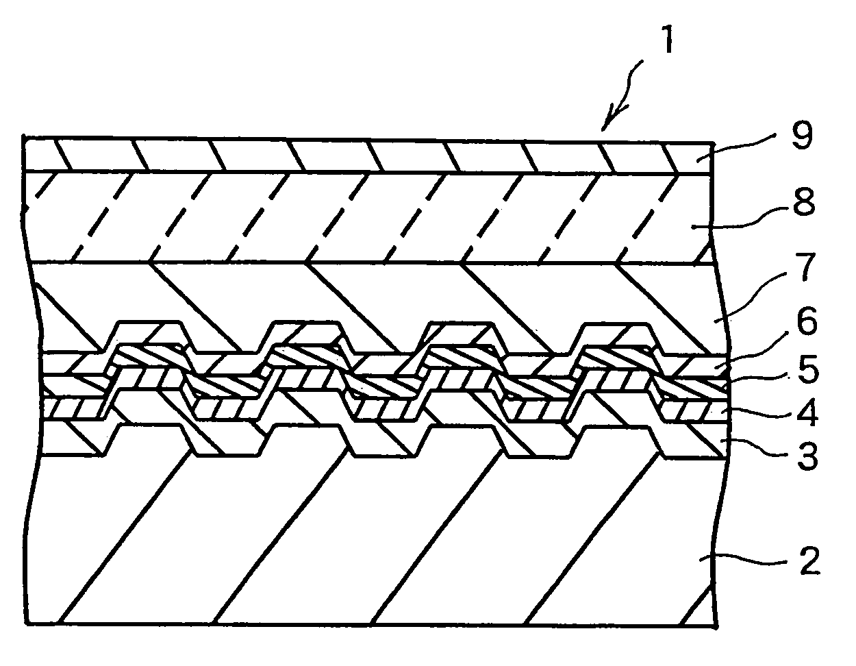
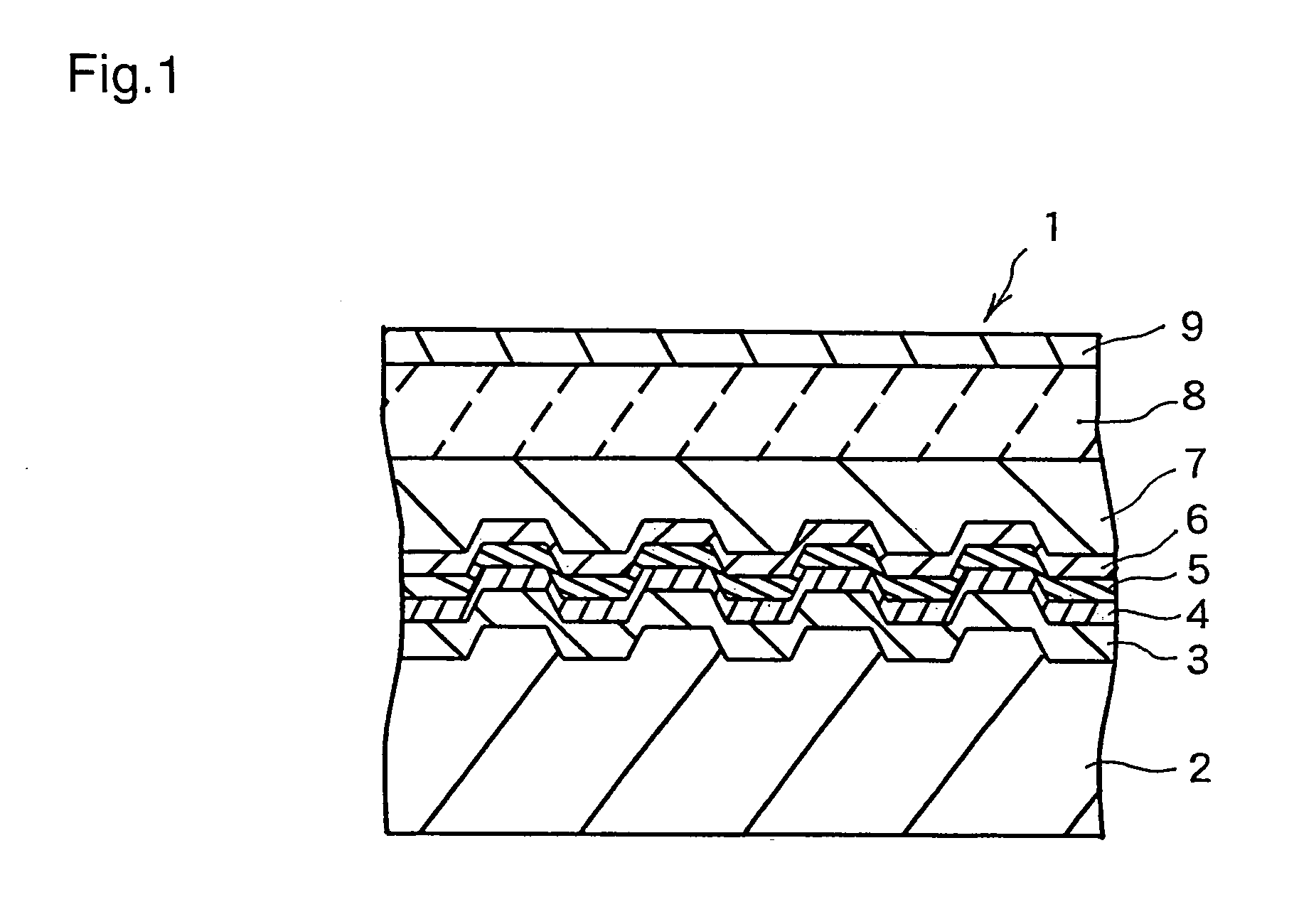
[0085]A sample optical recording disk having a layered structure as shown in FIG. 1 was prepared in the following manner.
[0086]A 100 nm thick reflective layer (3) of Al98Pd1Cu1 (in atomic ratio) was deposited on the surface of a grooved disk-shaped supporting substrate (2) (formed of polycarbonate, 120 mm in diameter and 1.2 mm in thickness) by sputtering. The depth of the above grooves, which is represented by light-path length at wavelength λ=405 nm, was set into λ / 6. The recording track pitch in the groove-recording scheme was set into 0.32 μm.
[0087]A 20 nm thick second dielectric layer (4) was then deposited on the surface of the reflective layer (3) by sputtering using an Al2O3 target. On the surface of the second dielectric layer (4), a 12 nm thick recording layer (5) was then deposited by sputtering using an alloy target formed of a phase-changing material. The composition of the recording layer (5) (in atomic ratio) was Sb74Te18 (Ge7In1). Sub...
PUM
| Property | Measurement | Unit |
|---|---|---|
| particle size | aaaaa | aaaaa |
| thickness | aaaaa | aaaaa |
| thickness | aaaaa | aaaaa |
Abstract
Description
Claims
Application Information
 - R&D
- Intellectual Property
- Life Sciences
- Materials
- Tech Scout
- Unparalleled Data Quality
- Higher Quality Content
- 60% Fewer Hallucinations
Browse by: Latest US Patents, China's latest patents, Technical Efficacy Thesaurus, Application Domain, Technology Topic, Popular Technical Reports.
© 2025 PatSnap. All rights reserved.Legal|Privacy policy|Modern Slavery Act Transparency Statement|Sitemap|About US| Contact US: help@patsnap.com


