
Field effect transistor semiconductor device

a semiconductor device and field effect technology, applied in the field of semiconductor devices, can solve the problems of device insufficiently achieving high-frequency characteristic and high-power characteristic, leakage current generation, and reducing thickness, and achieve the effect of facilitating the formation of via holes

Active Publication Date: 2006-07-18
PANASONIC CORP
View PDF13 Cites 45 Cited by
  • Summary
  • Abstract
  • Description
  • Claims
  • Application Information

AI Technical Summary

Benefits of technology

[0012]In view of the above-described problems, an object of the present invention is to prevent a leakage current produced between a substrate and a semiconductor layer and to facilitate formation of a via hole so that high-frequency characteristic and high-power characteristic are achieved in a semiconductor device including a Group III–V nitride semiconductor and having a via hole structure.

Problems solved by technology

First, due to an electric field applied between the substrate 101 and the semiconductor layer 102 including the active layer, a leakage current is produced between the substrate 101 and the semiconductor layer 102.
Secondly, SiC or sapphire used for the substrate 101 is normally very hard and highly resistant to chemicals; therefore, it is considerably difficult to form the via hole 106 in the substrate 101 made of SiC or sapphire so that the via hole 106 passes therethrough to reach the bottom surface of the substrate 101, while maintaining the strength of the substrate 101, i.e., while not reducing the thickness of the substrate 101. On the other hand, if the substrate 101 made of SiC or sapphire is polished to reduce its thickness and then the via hole 106 is formed, the substrate 101 whose thickness is reduced becomes fragile, and therefore, the situation where the substrate 101 is cracked in the step of forming the via hole 106 is brought about.
Accordingly, the semiconductor device connected to the bottom-surface electrode 107 through the conventional via hole presents the problem that the device cannot sufficiently achieve high-frequency characteristic and high-power characteristic.

Method used


Image

  • Field effect transistor semiconductor device
  • Field effect transistor semiconductor device
  • Field effect transistor semiconductor device

Examples


first embodiment

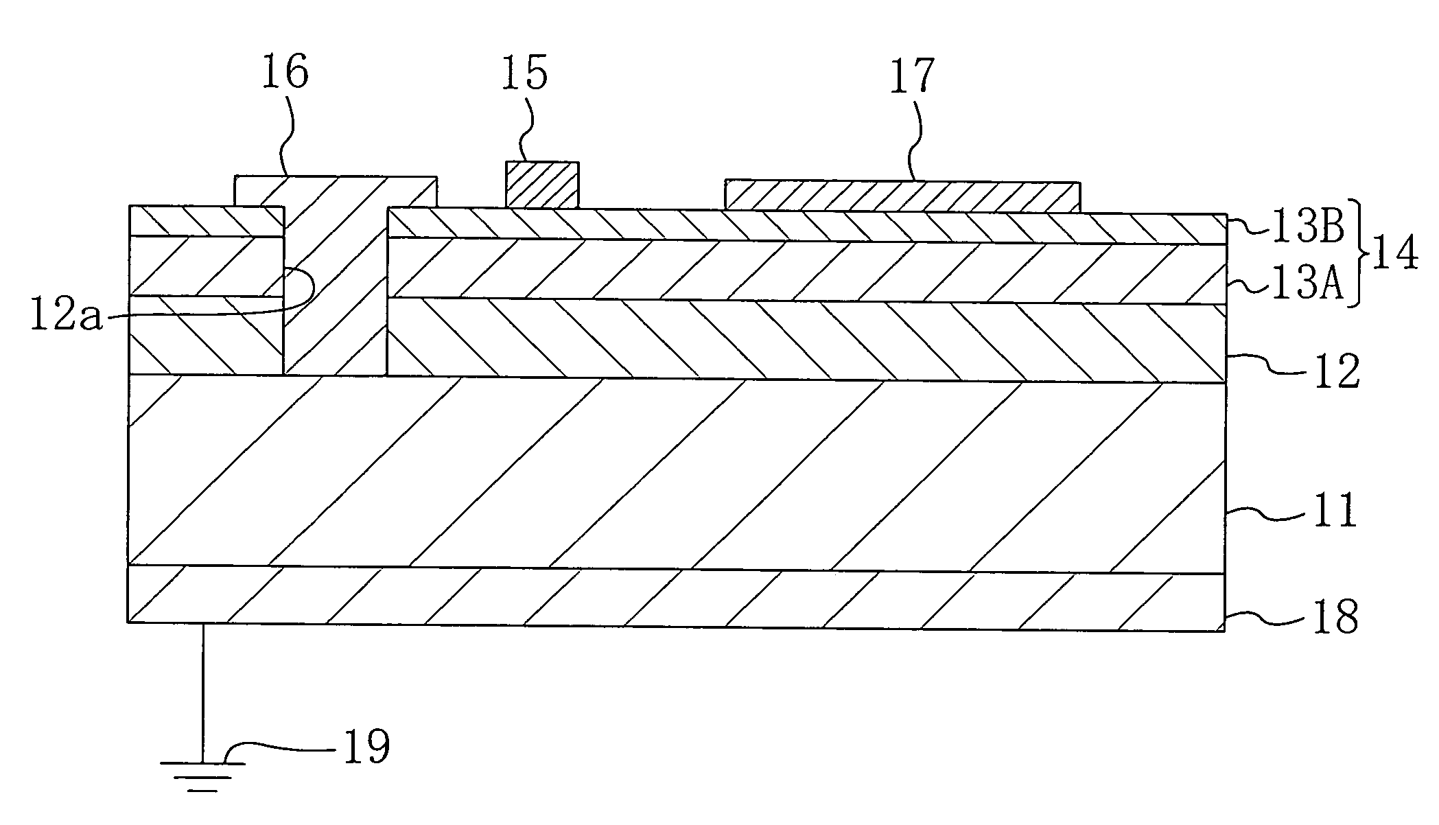
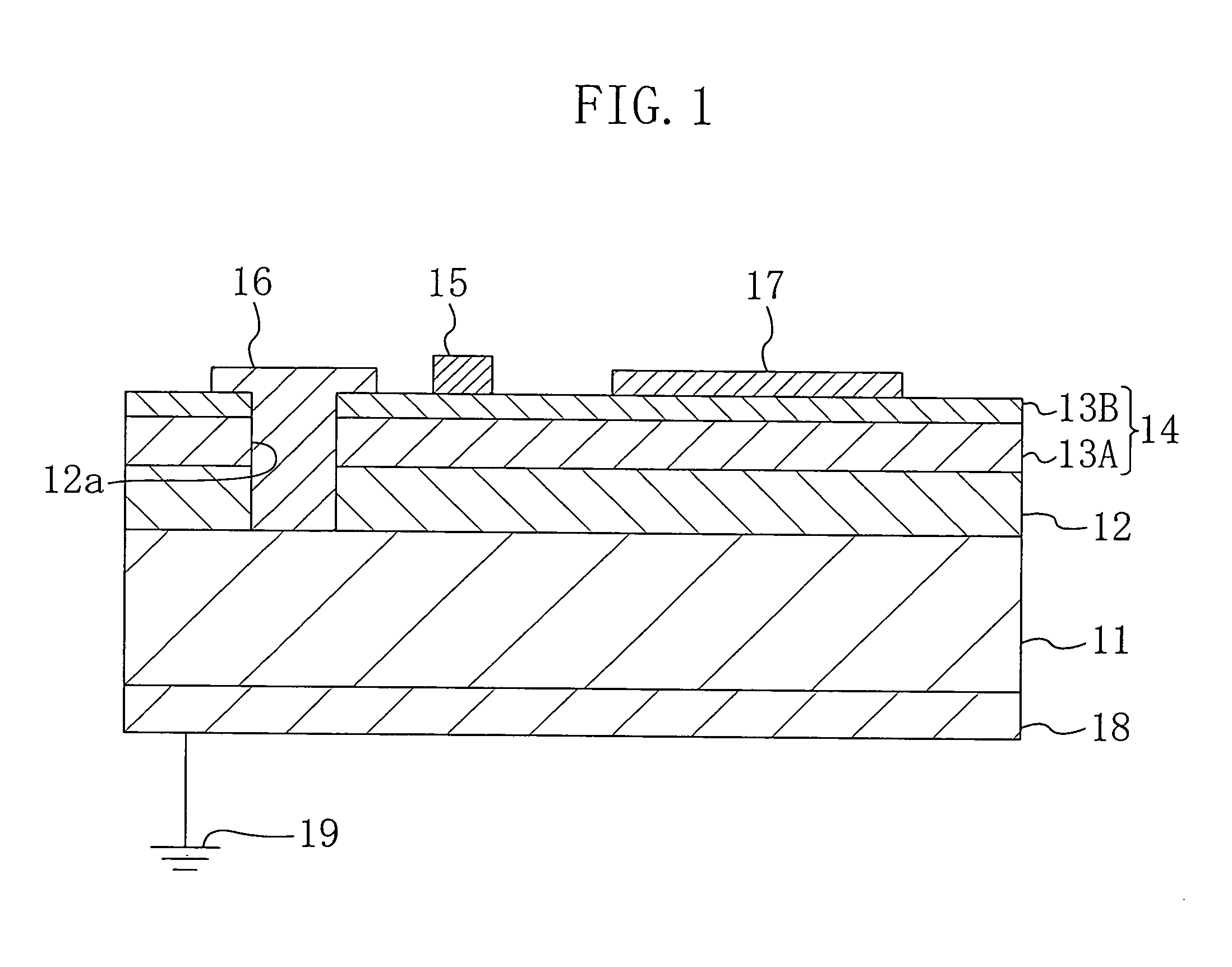
[0053]A first embodiment of the present invention will be described with reference to the associated drawing.

[0054]FIG. 1 illustrates a semiconductor device according to the first embodiment of the present invention, and schematically shows the cross section of a heterojunction field effect transistor (HFET). As shown in FIG. 1, the HFET according to the first embodiment includes: a P+-type conductive substrate 11 made of silicon (Si), for example; a buffer layer 12 as a first semiconductor layer made of a high resistance aluminum gallium nitride (AlxGa1-xN where 014 as a second semiconductor layer including a channel layer (active layer) and made of a Group III–V nitride semiconductor. In this embodiment, the conductive substrate 11 is formed so that a dopant concentration of phosphorus (P) or arsenic (As) becomes about 1×1020 cm−3 by ion implantation, for example. Further, the buffer layer 12 is formed so as to reduce lattice mismatch between the conductive substrate 11 and the el...

second embodiment

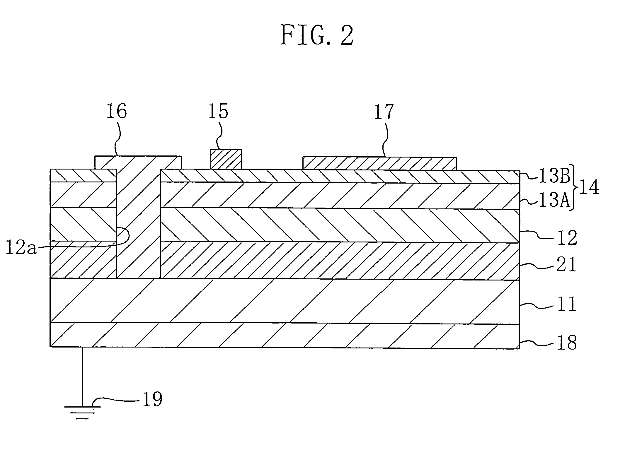
[0063]Hereinafter, a second embodiment of the present invention will be described with reference to the associated drawing.

[0064]FIG. 2 illustrates a semiconductor device according to the second embodiment of the present invention, and schematically shows the cross section of an HFET. In FIG. 2, the same constituting members as those shown in FIG. 1 are identified by the same reference characters, and thus the description thereof will be omitted.

[0065]As shown in FIG. 2, the HFET according to the second embodiment is provided, at its portion located between the P+-type conductive substrate 11 and the high resistance buffer layer 12, with at least one depletion-forming layer 21 as a third semiconductor layer which is made of P−-type silicon having a dopant concentration lower than that of the conductive substrate 11, i.e., a resistance higher than that of the conductive substrate 11. In this embodiment, the thicknesses of the high resistance buffer layer 12 and the depletion-forming ...

first modified example of second embodiment

[0069]FIG. 3 illustrates a semiconductor device according to a first modified example of the second embodiment of the present invention, and schematically shows the cross section of an HFET. In FIG. 3, the same constituting members as those shown in FIG. 2 are identified by the same reference characters, and thus the description thereof will be omitted.

[0070]In the first modified example, the depletion-forming layer 21 is formed so as to have a PN junction of a P-type lower layer 21a and an N-type upper layer 21b. In this case, the thicknesses of the high resistance buffer layer 12 and the depletion-forming layer 21, and the dopant concentrations of the lower layer 21a and the upper layer 21b are preferably set such that a maximum voltage, which can be supported by the buffer layer 12 and the depletion layer extended in the depletion-forming layer 21, becomes higher than a maximum voltage applied to the drain electrode 17.

[0071]Thus, due to the high resistance buffer layer 12 and th...


PUM


Abstract

A semiconductor device has: a buffer layer formed on a conductive substrate and made of AlxGa1-xN with a high resistance; an element-forming layer formed on the buffer layer, having a channel layer, and made of undoped GaN and N-type AlyGa1-yN; and a source electrode, a drain electrode and a gate electrode which are selectively formed on the element-forming layer. The source electrode is filled in a through hole provided in the buffer layer and the element-forming layer, and is thus electrically connected to the conductive substrate.

Description

BACKGROUND OF THE INVENTION[0001]The present invention relates to a semiconductor device including a Group III–V nitride semiconductor, and in particular relates to a field effect semiconductor device in which an electrode is provided on a bottom surface of a substrate.[0002]Group III–V nitride semiconductors such as gallium nitride (GaN), aluminum nitride (AlN) and indium nitride, i.e., a mixed crystal thereof represented by the following general formula: AlxGa1-x-yInyN (where 0≦x≦1, and 0≦y≦1), are examined not only for application to a short-wavelength optical device that utilizes a wide bandgap and a direct transition type band structure, which are physical properties of the mixed crystal, but also for application to an electron device because of the other properties of the mixed crystal such as a high breakdown electric field and a high saturation electron velocity.[0003]In particular, a heterojunction field effect transistor (hereinafter, will be called an “HFET”) that utilize...

Claims


Application Information

Patent Timeline
Patent Type & Authority Patents(United States)
IPC IPC(8): H01L31/0328H01L21/20H01L21/28H01L21/338H01L29/20H01L29/417H01L29/778H01L29/812H01S5/30
CPCH01L29/7787H01L29/41766H01L21/02425H01L21/02458H01L29/2003H01L21/0254H01L29/4175
Inventor MURATA, TOMOHIROHIROSE, YUTAKAIKEDA, YOSHITOTANAKA, TSUYOSHIINOUE, KAORUUEDA, DAISUKEUEMOTO, YASUHIRO
Owner PANASONIC CORP
Learn More