Ridge waveguide semiconductor laser diode

Inactive Publication Date: 2006-07-04
FURUKAWA ELECTRIC CO LTD
View PDF12 Cites 8 Cited by
  • Summary
  • Abstract
  • Description
  • Claims
  • Application Information

AI Technical Summary

Benefits of technology

[0014]It is another object of the present invention to provide a ridge waveguide semiconductor laser diode which is capable of operating with excellent stability in both of its transverse and longitudinal modes.
[0015]It is still another object of the present invention to provide a ridge waveguide semiconductor laser diode which is capable of operating with a FBG in a stable manner to provide a stable light source for the EDFA.
[0019]In accordance with the semiconductor laser diode of the present invention, due to the value for “D”, the kink phenomenon in the characteristic of the optical output power with respect to injected current caused by a beam steering phenomenon can be improved, as a result of which an excellent linear characteristic can be obtained in a higher output power range, whereby the ridge waveguide semiconductor laser diode can operate with excellent stability in the transverse and longitudinal modes. In addition, the potential for COD failure is significantly reduced.
[0020]If an FBG is positioned at the front facet of a GaAs-based quantum well laser diode according to the present invention, the GaAs quantum well laser diode operates in a stable output power, and can be used to construct an EDFA having excellent operational characteristics.

Problems solved by technology

The beam steering phenomenon is known in the art and it means that the light beam moves in the direction parallel to the active layers (as viewed from the front facet of the laser), which causes the characteristic of the optical output with respect to injected current in the semiconductor laser diode to be non-linear by having one or more kinks in the characteristic, thereby deteriorating the laser characteristic significantly.
Accordingly, signal conversion cannot be effected from the injected current due to the deteriorated laser characteristic.
For preventing the generation of the problem beam steering phenomenon in a high output power range, it is necessary to consider complicated and various effects, such as the waveguide mode control of the active layers, and thus the problem is not solved in the conventional GaAs quantum-well laser diode.
However, if a GaAs-based quantum-well laser diode having a lasing wavelength of 980 nm is used as a light source for an EDFA, the longitudinal mode operation is unstable when light returns from the FBG, whereby the optical output power fluctuates to cause another problem.
However, these problems are not peculiar to the GaAs-based quantum-well laser diode, but are common to general ridge waveguide semiconductor laser diodes.

Method used


Image

  • Ridge waveguide semiconductor laser diode
  • Ridge waveguide semiconductor laser diode
  • Ridge waveguide semiconductor laser diode

Examples


first embodiment

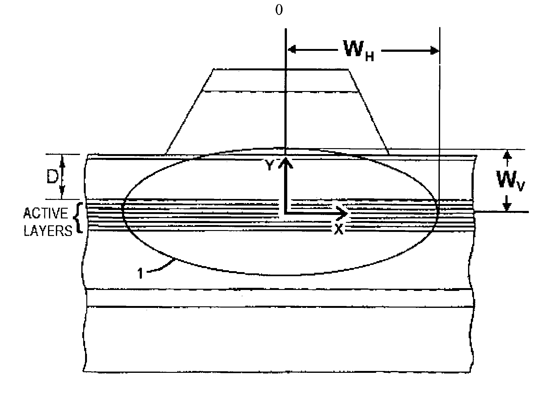
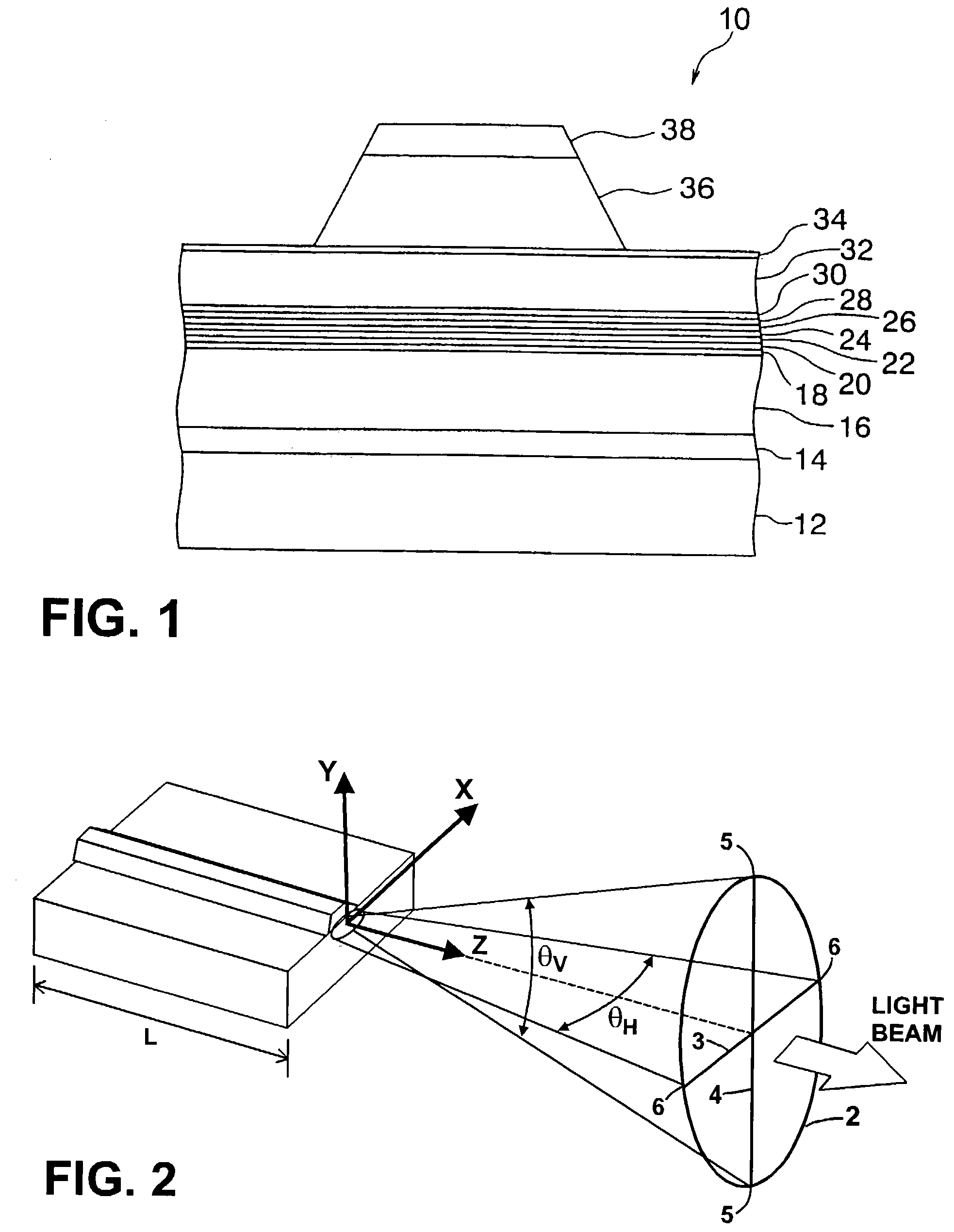
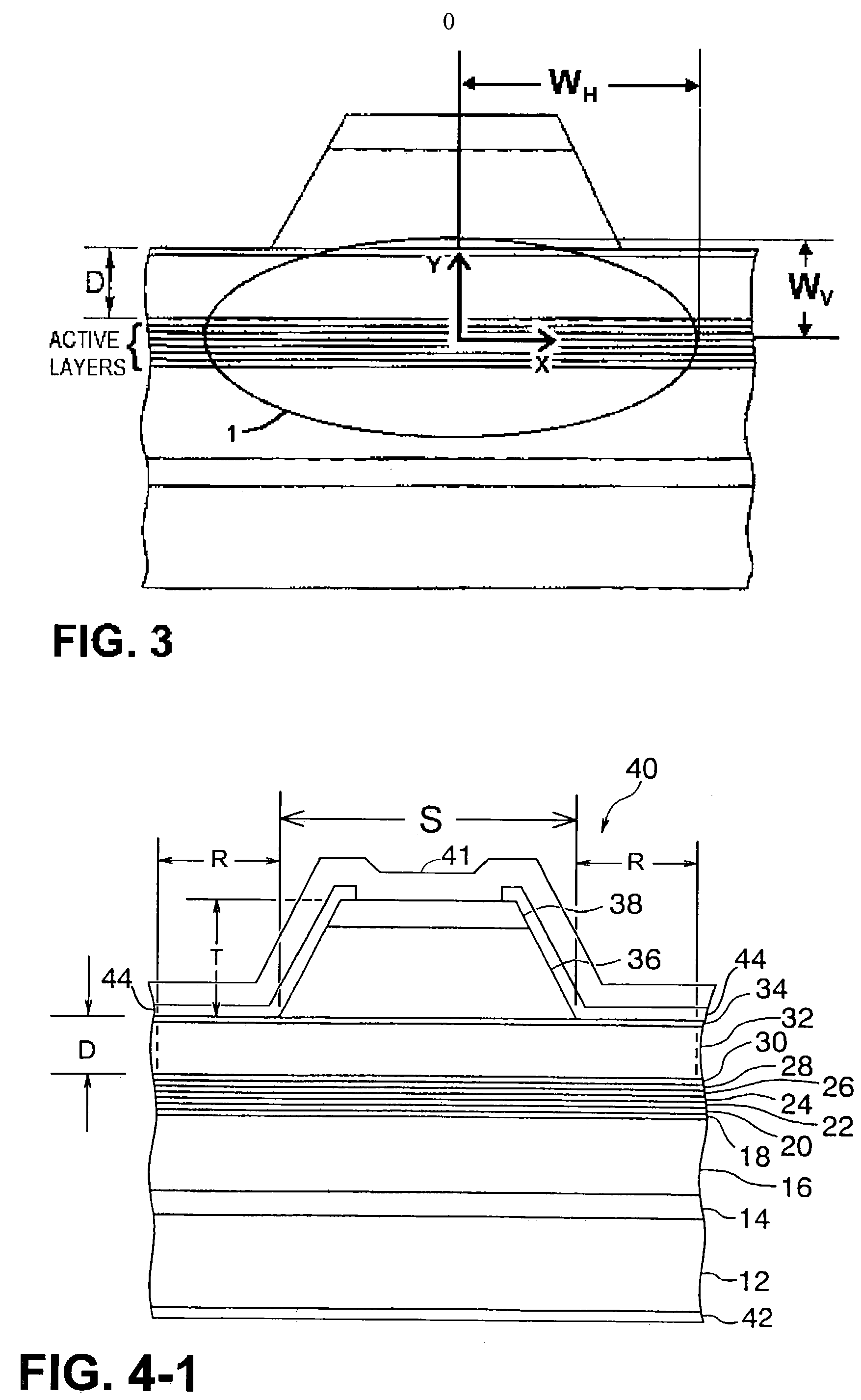
[0100]Referring to FIG. 4-1, a ridge waveguide semiconductor laser diode, generally designated by numeral 40, according to the present invention has a layer structure similar to the layer structure of the semiconductor laser 10 shown in FIG. 1 except that the overall remaining thickness D in the present embodiment, which is defined by the sum of thicknesses of the layers including the first upper cladding layer 32 and the etch stop layer 34, satisfies the following relationship:

1.10>D / W≧0.5.

[0101]The contents of the layers in the present embodiment are similar to those of the samples used in the first and second experiments.

[0102]More specifically, the laser diode 40 of FIG. 4-1 has a n-type GaAs substrate 12, and a layer structure grown thereon and including:[0103]n-GaAs buffer layer 14;[0104]n-Al0.3Ga0.7As lower cladding layer 16;[0105]Al0.2Ga0.8As first optical confinement layer 18;[0106]GaAs0.94P0.06 second optical confinement layer 20;[0107]In0.2Ga0.8As first strained quantu...

embodiment 220

[0133]The present invention may be practiced on a lasers made from a variety of compound-semiconductor material systems, emitting light over a broad wavelength spectrum, such as 700 nm to 1550 nm. Embodiments using the GaAs material system with an InGaAs well layer illustrated above with respect to FIG. 4-1 emit light at a wavelength of 980 nm or in a wavelength band around 980 nm, an example of such a band has a wavelength range from 850 nm to 1120 nm. In FIG. 13, we illustrate the formation of an embodiment 220 based on the InP material system, and which emits light at 1480 nm, or in a wavelength band near 1480 nm, an example of such a band has a wavelength range from 1300 nm to 1550 nm.

[0134]On the (100) surface of an n-InP substrate 201, the following layers are sequentially formed: an n-InP lower cladding layer 202 working as a buffer layer, a graded-index separate confinement heterostructure multi-quantum well (GRIN-SCH-MQW) active layer 203, a p-InP upper cladding layer 205, ...


PUM


Abstract

A GaAs based semiconductor laser having a combination of cladding layers including a ridge structure part, and a remaining part which overlays the active layers of the laser, and an etch stop layer sandwiched between the ridge structure part and the remaining part. The remaining part preferably overlies the entire surface of laser active layers and has a thickness “D” which satisfies 1.1×W>D≧0.5×W wherein W is the width of a spot size having a strength of 1 / e2 as measured at the laser front facet in a direction perpendicular to the active layers, wherein “e” is the base of the natural logarithm. The semiconductor laser solves the kink phenomenon to obtain an excellent linear relationship between the optical output power and the injected current.

Description

RELATED APPLICATIONS[0001]This application is a continuation-in-part of U.S. patent application Ser. No. 09 / 872,334, filed Jun. 1, 2001 now U.S. Pat. No. 6,618,417, which is a continuation-in-part of U.S. patent application Ser. No. 09 / 201,245, filed Nov. 30, 1998 now U.S. Pat. No. 6,560,260, the entire contents of the above-identified applications being incorporated herein by reference.FIELD OF THE INVENTION[0002]The present invention relates to a ridge waveguide semiconductor laser diode, and more particularly, to a ridge waveguide semiconductor laser diode having a high output power and an excellent laser characteristic and capable of operating at a higher output power with excellent stability.BACKGROUND OF THE INVENTION[0003]GaAs-based quantum-well laser diodes each having an InGaAs strained quantum-well active layer or layers, especially ridge waveguide semiconductor laser diodes, have been intensively researched and developed as feasible higher-output power semiconductor laser...

Claims


Application Information

Patent Timeline
IPC IPC(8): H01S5/00H01S5/22
CPCH01S5/22H01S2301/18
Inventor OHKUBO, MICHIOIKEGAMI, YOSHIKAZUNAMEGAYA, TAKESHIKASUKAWA, AKIHIKOYOSHIDA, JUNJI
Owner FURUKAWA ELECTRIC CO LTD
Why Eureka
Try Eureka