SCR-ESD structures with shallow trench isolation

a technology of trench isolation and scr, which is applied in the direction of semiconductor devices, semiconductor/solid-state device details, transistors, etc., can solve the problems of increasing the holding voltage, sti structure limiting effect on the current triggering and capacity of scr esd protection devices, and cataclysmic failures in these same circuits

Inactive Publication Date: 2006-06-13
TAIWAN SEMICON MFG CO LTD
View PDF10 Cites 8 Cited by
  • Summary
  • Abstract
  • Description
  • Claims
  • Application Information

AI Technical Summary

Benefits of technology

[0022]Accordingly, it is the primary objective of the invention to provide a novel, effective structure and manufacturable method for protecting ...

Problems solved by technology

The discharge of electrostatic energy from the human body or other sources known as electrostatic discharge (ESD) into the input or output pads of integrated circuit semiconductor devices has shown to cause catastrophic failures in these same circuits.
While providing good isolation properties, the STI structure has limiting effects on the current triggering and capacity of the SCR ESD protection devices.
This increases the holding voltage and trigger current of the lateral SCR, reduces lateral heat transfer capability, and possibly limi...

Method used


Image

  • SCR-ESD structures with shallow trench isolation
  • SCR-ESD structures with shallow trench isolation
  • SCR-ESD structures with shallow trench isolation

Examples


Embodiment Construction

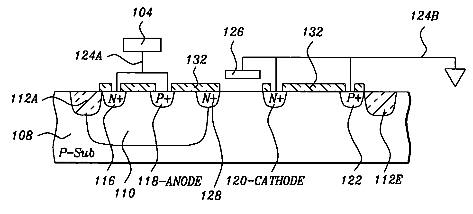
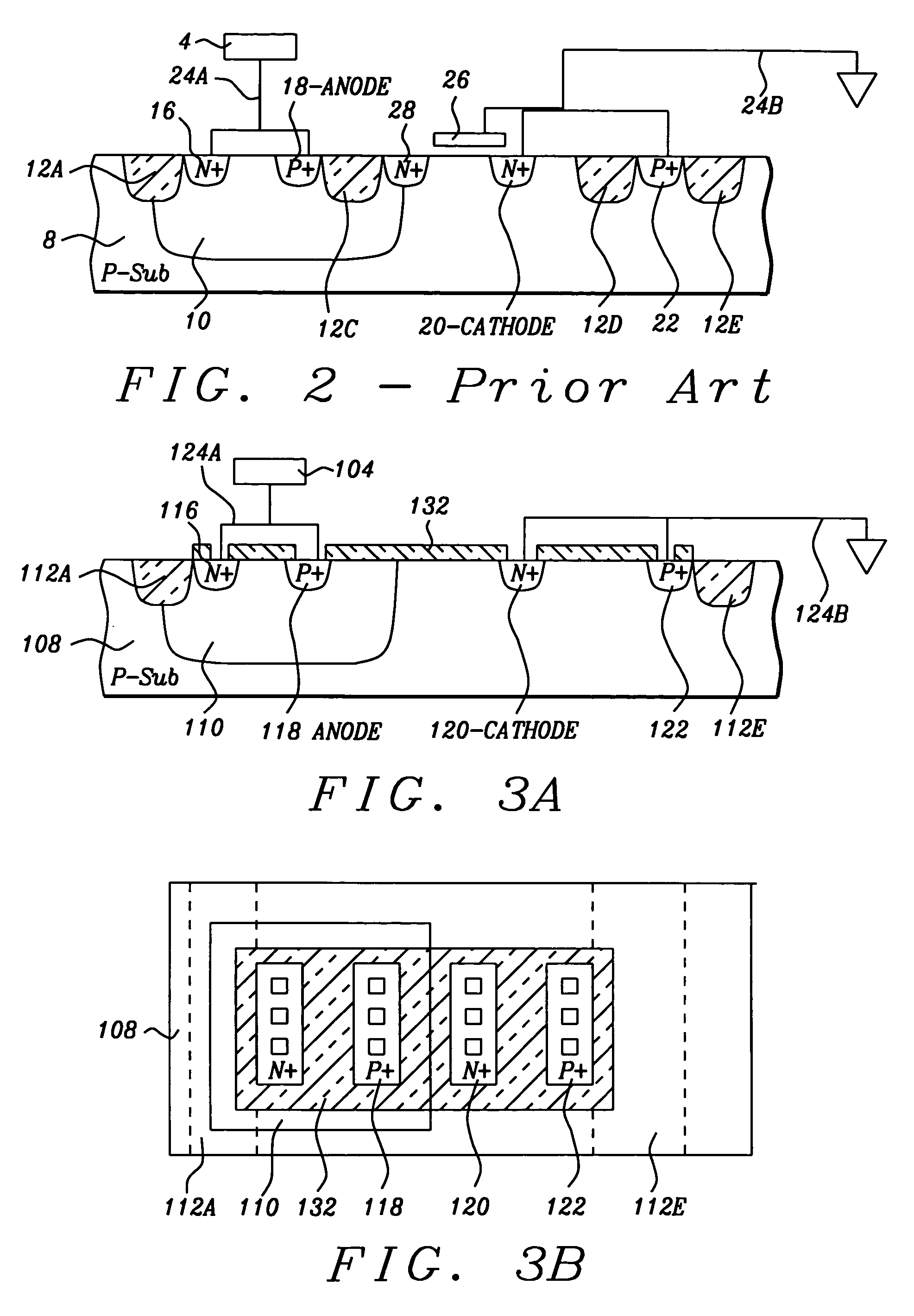
[0038]FIG. 3A shows a simplified cross section of one embodiment of the invention. A P doped substrate 108 with typical doping concentration of between 1E14 and 1E16 atoms / cm.sup.3 (a / cm.sup.3) contains an N-well 110 with a typical dopant concentration between 1E16 and 1E18 a / cm.sup.3. The N-well 110 is bounded at and near the surface by shallow trench isolation (STI) element 112A, typically between 0.2 to 1 um wide and 0.4 to 2 um deep. The STI element 112A is filled with a dielectric, typically silicon oxide (SiO.sup.2). Within the N-well 110 region are a N+ 116 and P+ 118 contact regions, with typical dopant concentrations of between 1E19 and 1E21 a / cm.sup.3. The N+ region 116 is bounded on the side away from the P+ contact region 118 by the STI 112A. The substrate 110 has N+ contact 120 and P+ contact 122, with a typical dopant concentration of between 1E19 and 1E21 a / cm.sup.3 of donor and receptor dopant respectively. The outside edge of substrate P+ contact 122 is bounded by S...


PUM


Abstract

A novel device structure and process are described for an SCR ESD protection device used with shallow trench isolation structures. The invention incorporates an SCR device with all SCR elements essentially contained within the same active area without STI elements being interposed between the device anode and cathode elements. This enhances ESD performance by eliminating thermal degradation effects caused by interposing STI structures, and enhances the parasitic bipolar characteristics essential to ESD event turn on. Enabling this unique design is the use of an insulation oxide surface feature which prevents the formation of contact salicides in unwanted areas. This design is especially suited to silicon-on-insulator design, as well as conventional SCR and LVTSCR designs.

Description

[0001]This is a division of patent application Ser. No. 10 / 189,874, filing date Jul. 5, 2002, now U.S. Pat. No. 6,720,622 Improved SCR-ESD Structures With Shallow Trench Isolation, assigned to the same assignee as the present invention.BACKGROUND OF THE INVENTION[0002](1) Field of the Invention[0003]The present invention relates generally to a structure and process for a semiconductor device which provides improved ESD protection for internal active semiconductor devices and more particularly to a semiconductor SCR like device which when used with shallow trench isolation, provides improved parasitic bipolar characteristics resulting in improved ESD protection performance.[0004](2) Description of Prior Art[0005]The discharge of electrostatic energy from the human body or other sources known as electrostatic discharge (ESD) into the input or output pads of integrated circuit semiconductor devices has shown to cause catastrophic failures in these same circuits. This is becoming more i...

Claims


Application Information

Patent Timeline
IPC IPC(8): H01L23/62H01L21/331H01L27/02H01L29/74
CPCH01L29/7436H01L27/0262
Inventor YU, TA-LEE
Owner TAIWAN SEMICON MFG CO LTD
Why Eureka
Try Eureka