Method of enlarging contact area of a gate electrode, semiconductor device having a surface-enlarged gate electrode, and method of manufacturing the same

a gate electrode and contact area technology, which is applied in the direction of semiconductor devices, electrical devices, transistors, etc., can solve the problems of polycide layer on the gate electrode, dopants diffraction to the edge portion, and the insufficient incorporation of the silicium layer into the gate electrode by heat treatment, so as to reduce the electrical resistance of the gate electrode

Inactive Publication Date: 2006-03-28
SAMSUNG ELECTRONICS CO LTD
View PDF2 Cites 4 Cited by
  • Summary
  • Abstract
  • Description
  • Claims
  • Application Information

AI Technical Summary

Benefits of technology

[0009]Accordingly, an object of the present invention is to provide a method of forming a gate electrode having a stable polycide layer and yet wherein overlay parasitic capacitance between the gate electrode and the substrate is minimal.
[0013]The thickness of the second insulating layer is preferably reduced by a chemical mechanical polishing (CMP) process followed by a wet-etch process. After the second conductive layer is formed on the second insulating layer and the gate pattern, the second conductive layer is selectively etched by an anisotropic etching process. As a result, the spacer formed by the conductive material at both sides of the upper portion of the gate pattern enlarges the surface area of the gate pattern.
[0019]Preferably, the main body and wings of the gate electrode comprise polysilicon, and the capacitance preventative layer is a low-temperature oxide (LTO). In addition, the semiconductor device of the present invention may further comprise an anti-diffusion layer for preventing ion dopants in the source / drain region of the substrate from diffusing into a channel region located beneath the gate electrode. The gate electrode preferably also comprises a metal silicide layer on the main body and wings thereof to thereby reduce the electrical resistance of the gate electrode. The metal silicide layer may also be disposed on the source / drain electrode to thereby reduce the electrical resistance thereof.

Problems solved by technology

Accordingly, the contact area between the gate electrode and the metal used to form the silicide layer is so small that the silicide layer is not sufficiently incorporated into the gate electrode by the heat treatment.
That is, when the line width is less than 0.13 μm, the resistance of the polycide layer on the gate electrode is unstable and hence, the polycide layer does not reduce the electrical resistance at the gate electrode.
However, the dopants diffuse to the edge portion of the gate electrode due to the heat.
Therefore, a time delay is produced according to the time it takes to charge the parasitic capacitor.
However, these techniques each fail to prevent the occurrence of a time delay due to the overlay parasitic capacitance between the gate electrode and substrate.

Method used


Image

  • Method of enlarging contact area of a gate electrode, semiconductor device having a surface-enlarged gate electrode, and method of manufacturing the same
  • Method of enlarging contact area of a gate electrode, semiconductor device having a surface-enlarged gate electrode, and method of manufacturing the same
  • Method of enlarging contact area of a gate electrode, semiconductor device having a surface-enlarged gate electrode, and method of manufacturing the same

Examples


Embodiment Construction

[0022]The present invention now will be described more fully hereinafter with reference to the accompanying drawings.

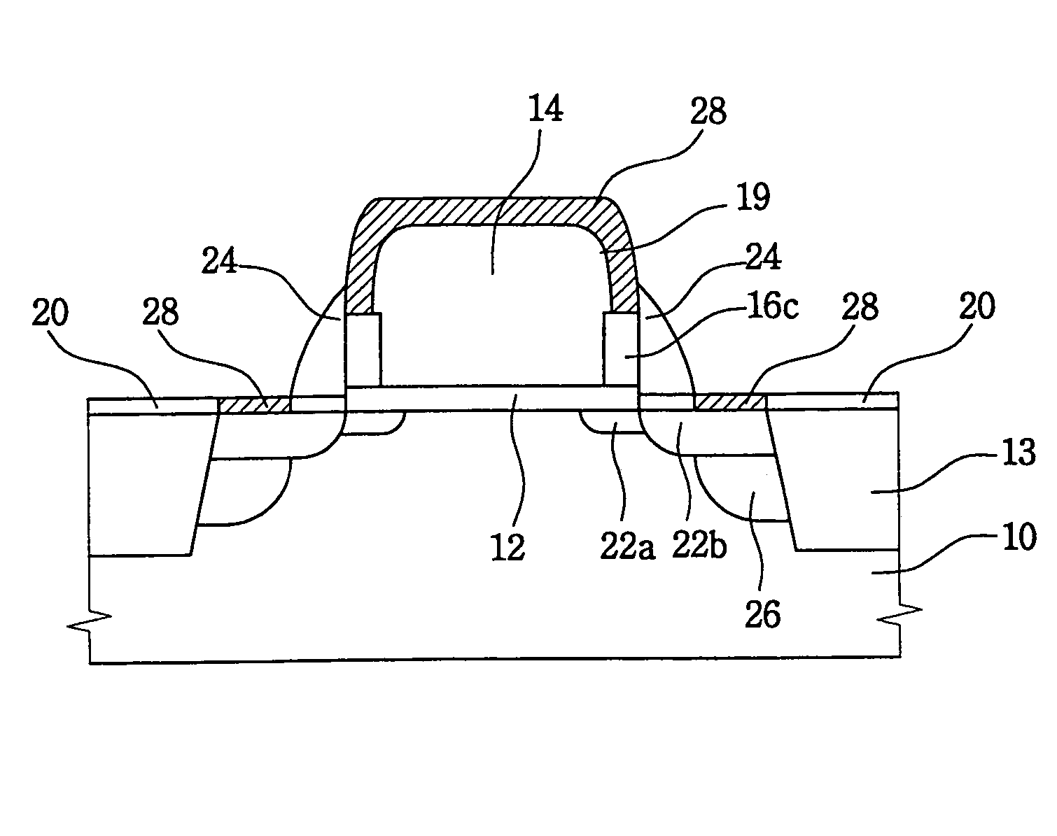
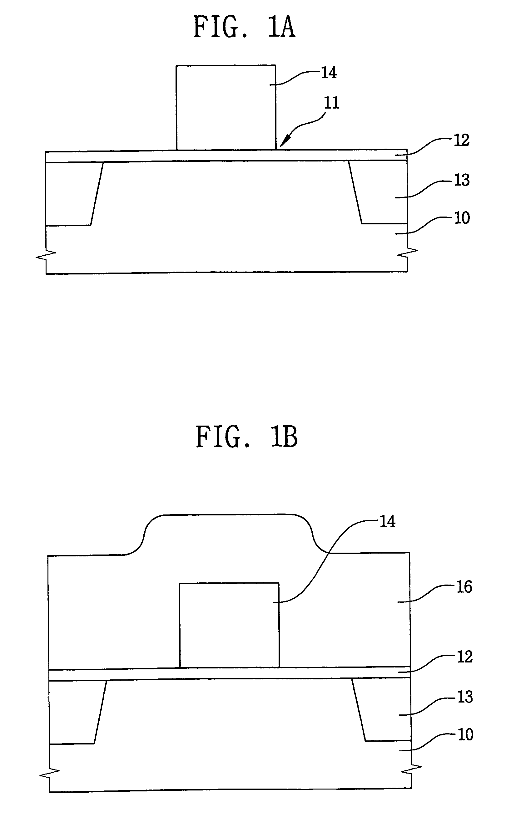
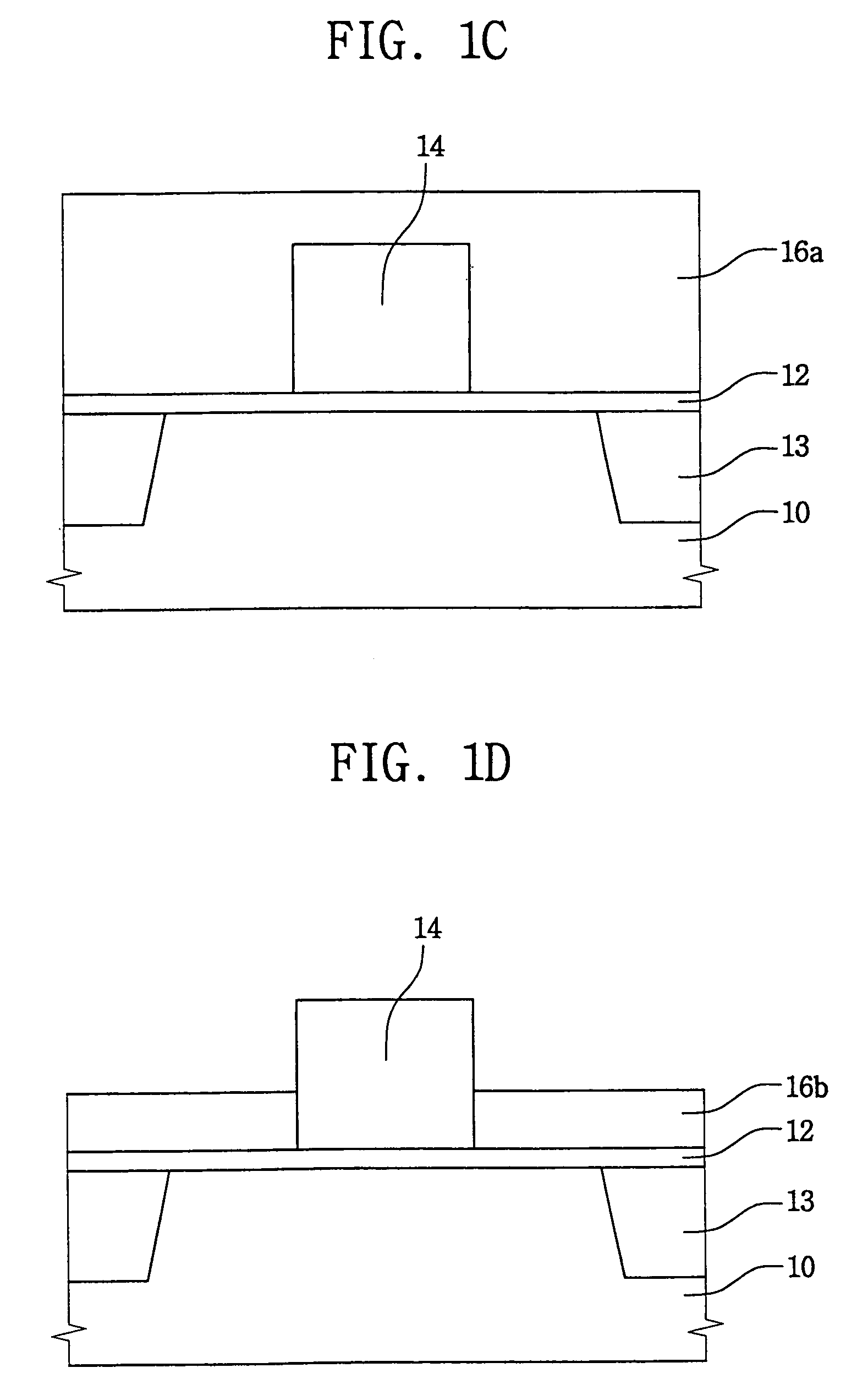
[0023]Referring first to FIG. 1A, at least one gate pattern 14 is formed on a semiconductor substrate 10 as follows. The substrate 10 is coated with a first insulating layer 12, i.e., a gate insulating layer, and then the substrate 10 is coated with a first layer (not shown) of conductive material. Next, the first conductive layer is patterned to thereby form the gate pattern 14 on the substrate 10. Therefore, the gate pattern 14 is electrically insulated from the substrate 10 by the first insulating layer 12. A plurality of transistors are disposed on the substrate 10, and are electrically isolated from each other by an isolation structure 13. The isolation structure 13 defines an active region 11 of the substrate 10 in which the transistors operate. Current cannot pass through the isolation structure 13, which constitutes a field region or a non-active region of a s...


PUM


Abstract

A highly integrated semiconductor device operates at a high speed due to low resistance at the gate electrode and minimal parasitic capacitance between the gate electrode and substrate. A gate pattern is formed on a substrate, and an insulating layer is formed over the substrate including over the gate pattern. The thickness of the insulating layer is reduced until the upper surface thereof beneath the level of the upper surface of the gate electrode. A conductive layer is then formed on the substrate, and is anisotropically etched to thereby form wings constituting a first spacer on upper sidewalls of the gate pattern. Then, the insulating layer is etched to leave a portion thereof beneath the wings. This remaining portion of the insulating layer constitutes a capacitance preventative layer that serves as a measure against the subsequent forming of a parasitic capacitor when source / drain electrodes are formed by implanting ions into the substrate and heat-treating the same.

Description

BACKGROUND OF THE INVENTION[0001]1. Field of the Invention[0002]The present invention relates to a semiconductor device having a mushroom- or T-shaped gate electrode, and to a method of fabricating the mushroom or T-shaped gate electrode. More specifically, the present invention relates to a semiconductor device having a gate electrode whose upper surface is relatively large so as to accommodate a metal silicide, and to a method of fabricating a gate electrode wherein the upper surface of the gate electrode is enlarged.[0003]2. Description of the Related Art[0004]Recent sub-micron integrated circuit technology aims at continuously reducing the line width and contact area of the semiconductor device, whereby the length of the gate lines of integrated circuits is continuously decreasing. In general, shortening the gate line increases the electrical resistance of the gate line (hereinafter, referred to as line resistance), resulting in a corresponding reduction in the operating speed o...

Claims


Application Information

Patent Timeline
Patent Type & Authority Patents(United States)
IPC IPC(8): H01L29/72H01L29/78H01L21/265H01L21/28H01L21/336H01L29/423
CPCH01L21/26506H01L21/26586H01L21/28052H01L21/28114H01L29/665H01L29/6656H01L29/6659H01L29/42376H01L29/7833H01L29/78
Inventor CHO, CHAN-HYUNGPARK, SUNG-GYU
Owner SAMSUNG ELECTRONICS CO LTD
Why Eureka
Try Eureka