Kinetic inductance for couplers and compact qubits
a coupler and kinetic technology, applied in the field of couplers, can solve the problems of josephson junctions being sensitive to local heating, devices prone to large variations, and other noises, and achieve the effect of minimising parasitic capacitan
- Summary
- Abstract
- Description
- Claims
- Application Information
AI Technical Summary
Benefits of technology
Problems solved by technology
Method used
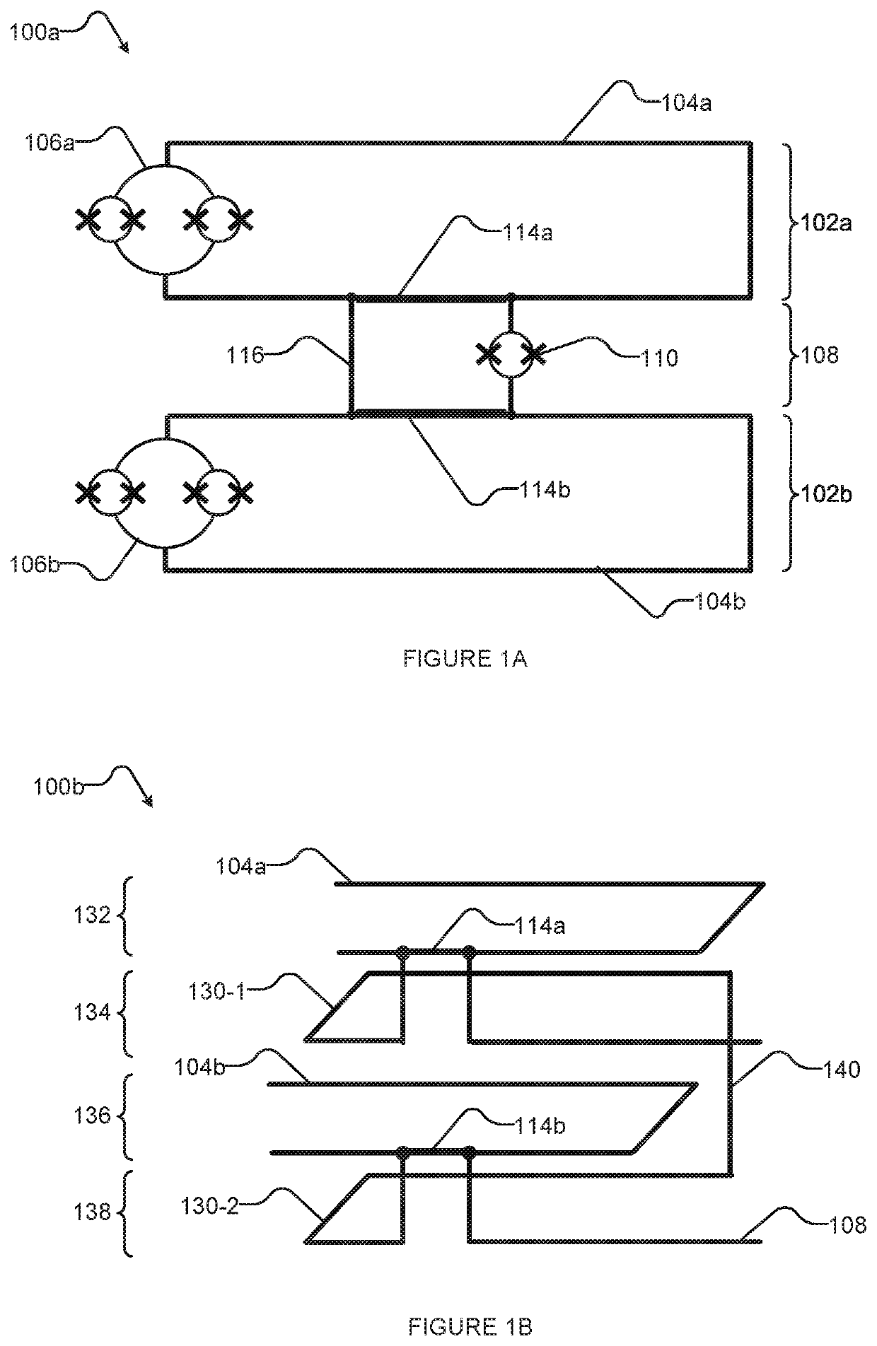
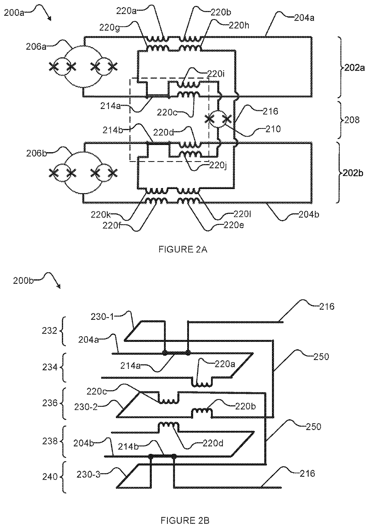
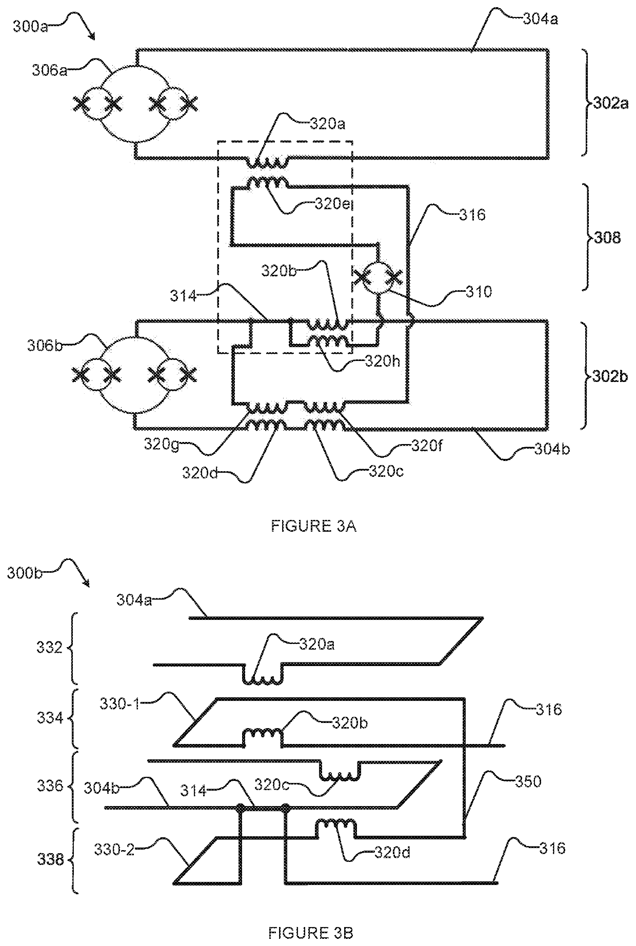
Image

Examples
Embodiment Construction
[0043]In the following description, certain specific details are set forth in order to provide a thorough understanding of various disclosed implementations. However, one skilled in the relevant art will recognize that implementations may be practiced without one or more of these specific details, or with other methods, components, materials, etc. In other instances, well-known structures associated with computer systems, server computers, and / or communications networks have not been shown or described in detail to avoid unnecessarily obscuring descriptions of the implementations.
[0044]Unless the context requires otherwise, throughout the specification and claims that follow, the word “comprising” is synonymous with “including,” and is inclusive or open-ended (i.e., does not exclude additional, unrecited elements or method acts).
[0045]Reference throughout this specification to “one implementation” or “an implementation” means that a particular feature, structure or characteristic de...
PUM
 Abstract
Description
Claims
Application Information
 - R&D
- Intellectual Property
- Life Sciences
- Materials
- Tech Scout
- Unparalleled Data Quality
- Higher Quality Content
- 60% Fewer Hallucinations
Browse by: Latest US Patents, China's latest patents, Technical Efficacy Thesaurus, Application Domain, Technology Topic, Popular Technical Reports.
© 2025 PatSnap. All rights reserved.Legal|Privacy policy|Modern Slavery Act Transparency Statement|Sitemap|About US| Contact US: help@patsnap.com