Positive-intrinsic-negative (PIN) diode array structure and manufacturing method thereof

A PIN diode and array structure technology, applied in the field of semiconductor integrated circuits, can solve the problems of high cost and large volume, achieve low cost, improve reverse isolation, and meet the effect of reverse isolation

Active Publication Date: 2013-04-24
SHANGHAI HUAHONG GRACE SEMICON MFG CORP
View PDF4 Cites 1 Cited by
  • Summary
  • Abstract
  • Description
  • Claims
  • Application Information

AI Technical Summary

Problems solved by technology

[0004] Conventional PIN diodes are mostly in the form of discrete devices. There are already packaged products on the market for sale. The disadvantage is that they need to be connected externally on the PCB, which is bulky and expensive.

Method used


Image

  • Positive-intrinsic-negative (PIN) diode array structure and manufacturing method thereof
  • Positive-intrinsic-negative (PIN) diode array structure and manufacturing method thereof
  • Positive-intrinsic-negative (PIN) diode array structure and manufacturing method thereof

Examples


Embodiment Construction

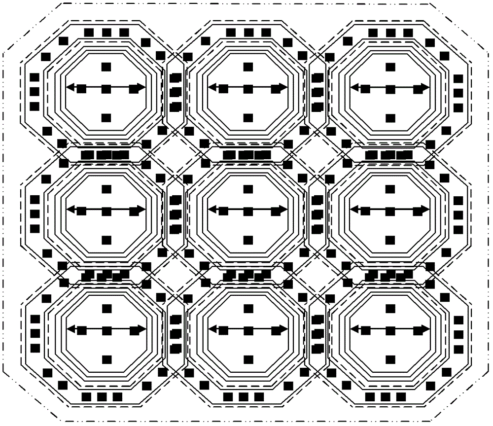
[0027] The PIN diode array structure of the present invention is composed of a plurality of PIN diode single tubes connected in parallel, and each PIN diode single tube includes a substrate 1, an N-type cathode 2, an intrinsic semiconductor 3, a P-type anode 7, an isolation region 4, an N-type outer base cathode 5. In order to minimize the parasitic capacitance, the array formed in parallel is preferably or close to a square, such as figure 2 As shown in the top view of the array structure, the array structure has 9 PIN diode single tubes forming a 3×3 square array, and adjacent PIN diode single tubes share the N-type outer base region cathode 5 .

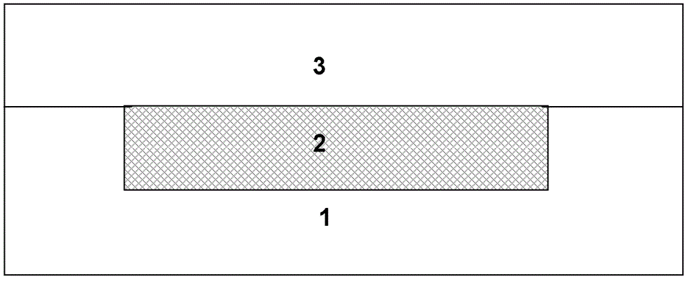
[0028] A disc-shaped N-type cathode 2 is formed above the substrate 1, an intrinsic semiconductor 3 with a thickness of 1.2 μm to 3 μm is grown above the middle part of the disc-shaped N-type cathode 2, and the peripheral part of the disc-shaped N-type cathode 2 is An annular N-type extrinsic base cathode 5 coaxial with the disk-...


PUM


Abstract

The invention discloses a positive-intrinsic-negative (PIN) diode array structure. The structure is formed by a plurality of PIN diodes which are connected in parallel. The each PIN diode comprises a substrate, an N type cathode, an intrinsic semiconductor, a P type anode, an isolation region and an N-type outer-base-region cathode. The N type cathode which is in a round sheet shape is formed above the substrate. The 1.2 micron-3 micron intrinsic semiconductor is grown above a middle portion of the N type cathode with the round sheet shape. The N-type outer-base-region cathode with an annular shape is formed above a peripheral portion of the N type cathode with the round sheet shape. The P type anode with the round sheet shape is formed above a central area of the intrinsic semiconductor which is far from an N type cathode terminal. The invention also discloses a manufacturing method of the PIN diode array structure. According to the invention, through increasing a thickness of an epitaxial layer and reducing leakage of electricity during reverse bias, reverse isolation of a large signal is improved when a reverse bias voltage is increased. A stray capacitance is minimized through a parallel connection of same units and design optimization. A small positive series resistance and the positive and negative stray capacitances are obtained so as to reduce positive insertion losses.

Description

technical field [0001] The invention relates to the field of semiconductor integrated circuits, in particular to a PIN diode array with high isolation and low insertion loss compatible with bipolar technology and a manufacturing method thereof. Background technique [0002] Typical applications for RF electronic switches are wireless transceivers. wireless transceivers such as figure 1 As shown, it usually consists of the following four parts: power amplifier (PA), low noise amplifier (LNA), radio frequency electronic switch, and logic control circuit. The power amplifier and the low noise amplifier are connected to the antenna through a radio frequency electronic switch to transmit and receive radio frequency signals. Since the signal transmitted from the power amplifier to the antenna must be strong enough, the RF electronic switch connected to it needs to have as low a forward conduction loss as possible. For low noise amplifiers, the signal from the power amplifier wi...

Claims


Application Information

Patent Timeline
Patent Type & Authority Applications(China)
IPC IPC(8): H01L27/082H01L29/868H01L29/06H01L21/8222
Inventor 周正良李昊
Owner SHANGHAI HUAHONG GRACE SEMICON MFG CORP
Why Eureka
Try Eureka