Method and apparatus for monitoring materials used in electronics
- Summary
- Abstract
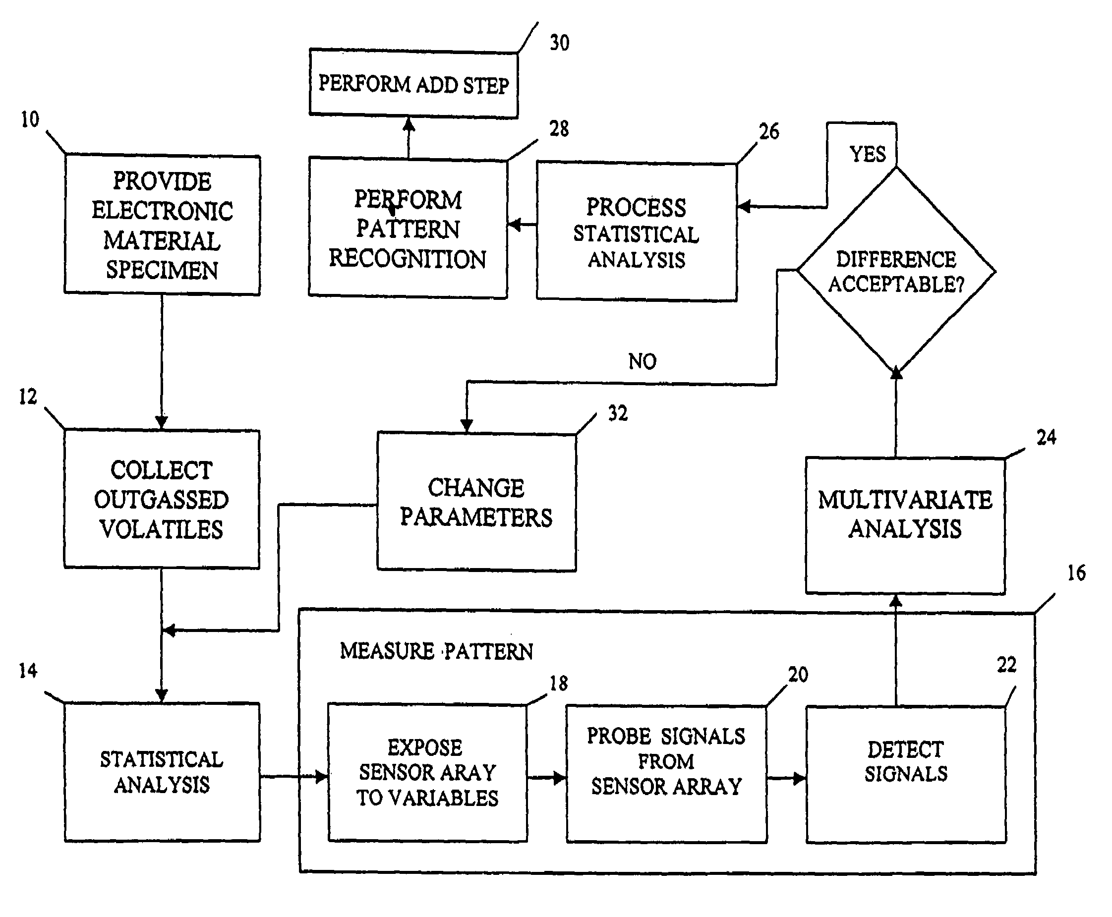
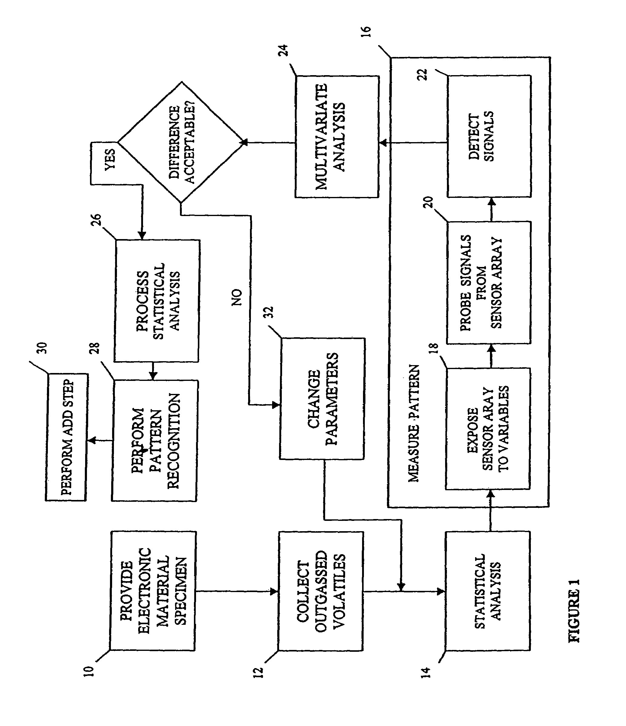
- Description
- Claims
- Application Information
AI Technical Summary
Benefits of technology
Method used
Image

Examples
example i
Analysis of Circuit Boards
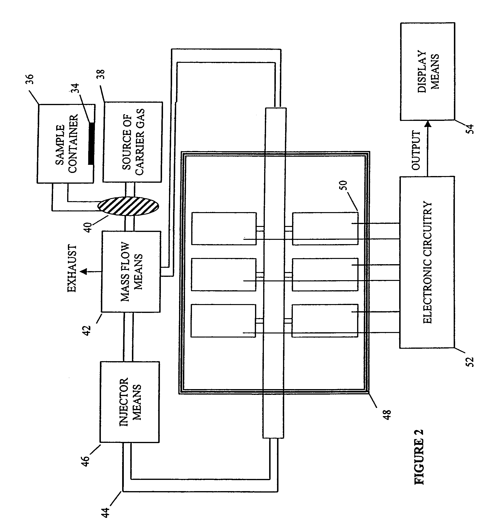
[0092]Several types of electronic components were analyzed by using a commercially available gas sensor array system (e.g. Prometheus system including mass spectrometer and 12 different metal oxide sensors, Alpha-M.O.S, New-Jersey, USA) equipped with a headspace autosampler (HS100, CTC, Switzerland) and an air conditioning unit (ACU500, Alpha-M.O.S, New Jersey, USA). The electronic component specimens were general purpose PC boards (i.e. epoxy glass based circuit boards), semiconductor logic device (e.g. CMOS dual decoder / demultiplexer) and transistors (e.g. NPN silicon). All samples were weighted (e.g. mass of 1 g) and directly disposed into 20 ml glass vials hermetically sealed with septum caps. The vials were loaded onto a tray of the headspace autosampler for which the following parameters were set; 10 minutes of incubation time in oven at 85° C. with 500 rpm agitation speed, 3 ml headspace capture for injection at 2.5 ml / s into the gas sensing analyzer...
PUM
 Abstract
Description
Claims
Application Information
 - R&D
- Intellectual Property
- Life Sciences
- Materials
- Tech Scout
- Unparalleled Data Quality
- Higher Quality Content
- 60% Fewer Hallucinations
Browse by: Latest US Patents, China's latest patents, Technical Efficacy Thesaurus, Application Domain, Technology Topic, Popular Technical Reports.
© 2025 PatSnap. All rights reserved.Legal|Privacy policy|Modern Slavery Act Transparency Statement|Sitemap|About US| Contact US: help@patsnap.com