Extreme UV light source and semiconductor exposure device

a light source and exposure device technology, applied in the field of extreme uv light source and semiconductor exposure device, can solve the problems of increasing the load of the evacuation pump, the inability of the optical system to use the optical system, and the inability to build a semiconductor exposure device which will withstand practical use in the industry, etc., and achieves a large absorption cross-sectional area and increased radiation density.

Inactive Publication Date: 2005-11-15
USHIO DENKI KK
View PDF5 Cites 4 Cited by
  • Summary
  • Abstract
  • Description
  • Claims
  • Application Information

AI Technical Summary

Benefits of technology

[0021]The invention was devised to push the above noted upper boundary higher. Thus, a primary object of the present invention is to devise an extreme UV light source in which the emission of extreme UV radiation with a wavelength of 13.5 nm with increased radiation density is enabled without increasing the pressure of Xe with a large absorption cross-sectional area of photons of 13.5 nm light.
[0026]By mixing in such a substance, it is expected that ionization of the Xe ions into a stage with a higher dimension (charging) will be suppressed so that, in this way, the temperature at which the particle density of the 10-valent ions (Xe10+) is maximum, will be shifted to a higher temperature and that the radiation density of the extreme UV light increased.
[0030]Furthermore, if the average atomic density of Xe in a narrow, small passage is at least 2.4×10¹⁶ / cm3 (2.4×10²² / m3), a state with a high ion density is obtained, by which a three-body collision in which electrons are involved as two bodies can be easily formed. In this way, ionization of the Xe ions is suppressed, and the temperature at which the particle density of the 10-valent Xe ions (Xe10+) is maximum is shifted to a higher temperature, by which the radiation density of the extreme UV light increases.

Problems solved by technology

However, in the case of using light with a wavelength of 13.5 nm (hereinafter called “13.5 nm light”) for purposes of semiconductor exposure, optical lenses cannot be used for the optical system.
Without an extreme UV radiation light source with high radiation density, the possibility of building a semiconductor exposure device which will withstand practical use in industry is low.
Therefore, it becomes necessary to evacuate excess Xe with an evacuation pump and to reduce the Xe in the space from the vicinity of the open end of the capillary (narrow, small passage) up to the irradiated surface; this leads to an increase of the load of the evacuation pump (enlargement).
As a result, the extreme UV light source becomes larger; this is considered disadvantageous with respect to the arrangement of the device.
If an evacuation system with an excessively high evacuation rate is used, the Xe pressure in the discharge part also decreases, resulting in the disadvantage that a reduction of the radiation density is induced.
This means that, under certain conditions of atomic density, a maximally high radiation density is fixed, and it is not possible to go higher.

Method used


Image

  • Extreme UV light source and semiconductor exposure device
  • Extreme UV light source and semiconductor exposure device
  • Extreme UV light source and semiconductor exposure device

Examples


Embodiment Construction

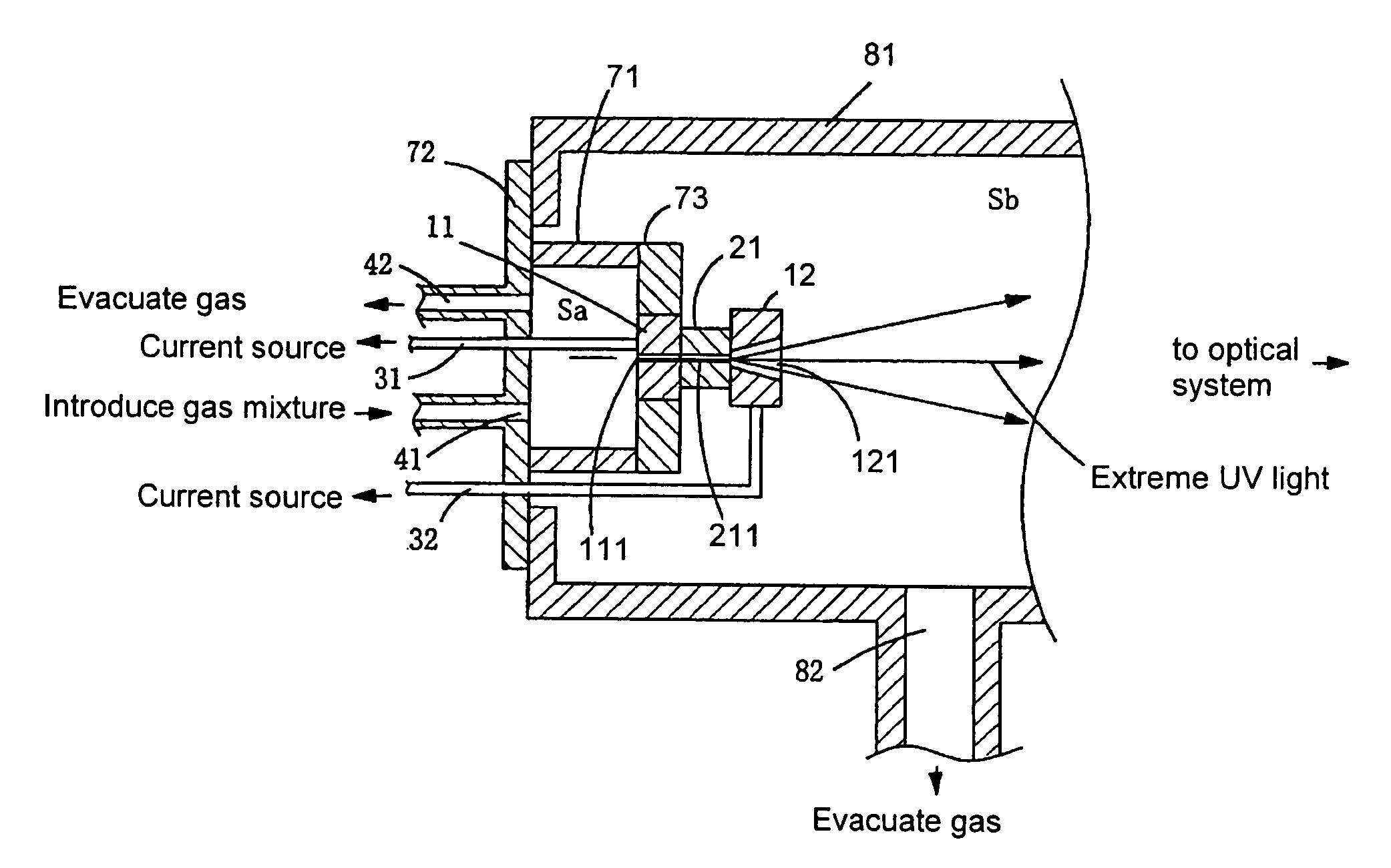
[0058]FIG. 1 is a schematic of one example of an arrangement of an extreme UV light source using a capillary discharge with which the invention is used. FIG. 1 is a cross section which is cut by a plane which passes through the optical axis of the extreme UV light which is emitted from the extreme UV light source.

[0059]As is shown in FIG. 1, between the first electrode 11 and the second electrode 12, for example, of tungsten, there is a capillary body 21 which is a cylindrical insulation body which is made, for example, of silicon nitride or the like and which has a capillary 211 with a diameter of 3 mm in the middle. The material for the electrodes 11, 12 can also be tantalum. The material for the capillary body 21 can also be aluminum nitride or diamond.

[0060]A current source (not shown) is electrically connected to the first electrode 11 and the second electrode 12 via electrical lines 31, 32. Between the first electrode 11 and the second electrode 12, a high voltage is applied i...


PUM


Abstract

A UV light source in which Xenon (Xe) gas is mixed with a substance which, in the temperature range in which 10-valent Xe ions (Xe10+) occur, emits a number of free electrons from a molecule or an atom that at least half the number of electrons which are released from a Xe atom, and which at room temperature is molecular or atomic (for example Ar, Kr, Ne, N2 and NH3). A high voltage is applied in a pulse-like manner to the electrode on the ground side and the electrode on the high voltage side to produce a plasma with a high temperature and from which extreme UV light with a wavelength of 13.5 nm is formed and emitted. The invention can also be used an extreme UV light source of the capillary, plasma focus, and Z pinch types for example.

Description

BACKGROUND OF THE INVENTION[0001]1. Field of the Invention[0002]The invention relates to an extreme UV light source which is used as the light source of a device for a semiconductor exposure device, and a semiconductor exposure device using this light source. The invention relates especially to an extreme UV light source for which the radiation density of this light source can be increased, and a semiconductor exposure device.[0003]2. Description of the Prior Art[0004]The refinement of circuit parts of components has been continuing recently for purposes of increasing the efficiency of the semiconductor components and reducing their costs.[0005]To do this, the wavelengths of a light source for pattern reduction exposure using light are becoming increasingly shorter. It is proposed that, instead of laser light with wavelengths of roughly 200 nm which is currently being used, extreme UV radiation with a wavelengths of 13.5 nm be used for purposes of semiconductor exposure as the light...

Claims


Application Information

Patent Timeline
IPC IPC(8): H05G2/00G21K5/04G21K5/00G03F7/20G21K1/00G21K5/02H01L21/027H05H1/06H05H1/24
CPCH05G2/003H05G2/006
Inventor HIRAMOTO, TATUMI
Owner USHIO DENKI KK
Why Eureka
Try Eureka