Encapsulants for protecting MEMS devices during post-packaging release etch

Inactive Publication Date: 2005-10-18
NAT TECH & ENG SOLUTIONS OF SANDIA LLC
View PDF9 Cites 201 Cited by
  • Summary
  • Abstract
  • Description
  • Claims
  • Application Information

AI Technical Summary

Benefits of technology

[0019]The present invention relates to methods to protect a MEMS or microsensor device through one or more release or activation steps in a “package first, release later” manufacturing scheme. This method of fabrication permits wirebonds, other interconnects, packaging materials, lines, bond pads, and other structures on the die to be protected from physical, chemical, or electrical damage during the release etch(es) or other packaging steps. Metallic structures (e.g., gold, aluminum, copper, nickel) on the device are also protected from galvanic attack because they are protected from contact with HF or HCL acids used for release etch(s).
[0021]In another embodiment, as much of the packaged, but not yet released, device as desired is coated with a photoimagable, liquid encapsulant having a low viscosity (e.g., SU-8). The surplus thickness of the low-viscosity encapsulant (which can be warmed to further lower its viscosity) is drained off the part, leaving a thin, substantially conformal, electrically insulating coating. The region over the active area is easily photodefined and then removed. Then the device is released with known release / coat / dry techniques.
[0022]Certain embodiments of the present invention employ a thin dielectric film, which may (e.g., SU-8) or may not be photoimageable (e.g., parylene). This dielectric material substantially conforms to the contour of wires or other interconnects, and provides an opportunity to shield signal and power lines by subsequently overcoating with a conductive metallic coating.
[0023]Use of a protective coating covering the passive area, but not covering the active area, reduces concerns about what materials are used in “package first, release later” packaging schemes, because release etchant (s) never comes in contact with these materials. It effectively renders all materials immune to release etch(s).

Problems solved by technology

Conventional electronic packaging methods, although expensive, are not presently adequate to carry these designs to useful applications with acceptable yields and reliability.
Unfortunately, probed “good” MEMS devices are then lost in significant quantity due to damage during subsequent packaging steps.
They can be easily damaged because they are unprotected (e.g. released).
Potential risks to the delicate released MEMS elements include electrostatic effects, dust, moisture, contamination, handling stresses, and thermal effects.
For example, ultrasonic bonding of wirebond joints can impart harmful vibrations to the fragile released MEMS elements.
In the case of microsensors, the active sensing elements (e.g., chemically reactive films), may be damaged if exposed prematurely during the packaging process.
Some problems exist with the use of wet acid etchants for releasing MEMS devices.
There are safety and environmental disposal issues with using strong acids like HF and HCL.
Also, the acid can attack and damage other features on the microelectronic device, including metal traces, lines, structures, films, bond pads, routing lines between bond pads, wirebonds, solder bumps, ring seals, bond interfaces, metallized layers, sensing materials, integrated circuits, such as CMOS or Bipolar structures and other semiconductor materials (e.g., standard photoresist protection used on CMOS or Bipolar chips may not provide sufficient protection from attack by acid etchants).
Use of wet release etchants can also damage other fragile structures due to hydrodynamic forces, including alignment marks, logos, and test structures, wirebonds (e.g., due to wire sweep).
Also, unprotected metallic structures (e.g., gold, aluminum, copper) on the device can be corroded by galvanic attack of the HF-bearing or HCL-bearing release solution.
This eliminates the above-mentioned problems with using a liquid etchant, but is typically a slower process.
However, such relatively thick protective coatings cannot be applied to released MEMS elements (or to exposed microsensing elements), because the coating would prevent the MEMS elements from moving (or, for example, prevent diaphragms or membranes in a pressure-sensitive element from flexing).
However, because of their high viscosity (from 1000–17,000 cts), delicate wirebonds can be damaged due to excessive wire sweep caused by high viscous shear forces applied during deposition of the photoresist (e.g., during spin coating).
Also, problems can exist from excessive electromagnetic cross-talk interference between neighboring conductors (signal lines, power lines, wirebonds, etc.) because they are electromagnetically unshielded from each other.
A thin, metallic overcoat could act as an electromagnetic shield, but this would also short-circuit the device since the exposed metallic conductors are not electrically insulated.

Method used


Image

  • Encapsulants for protecting MEMS devices during post-packaging release etch
  • Encapsulants for protecting MEMS devices during post-packaging release etch
  • Encapsulants for protecting MEMS devices during post-packaging release etch

Examples


Embodiment Construction

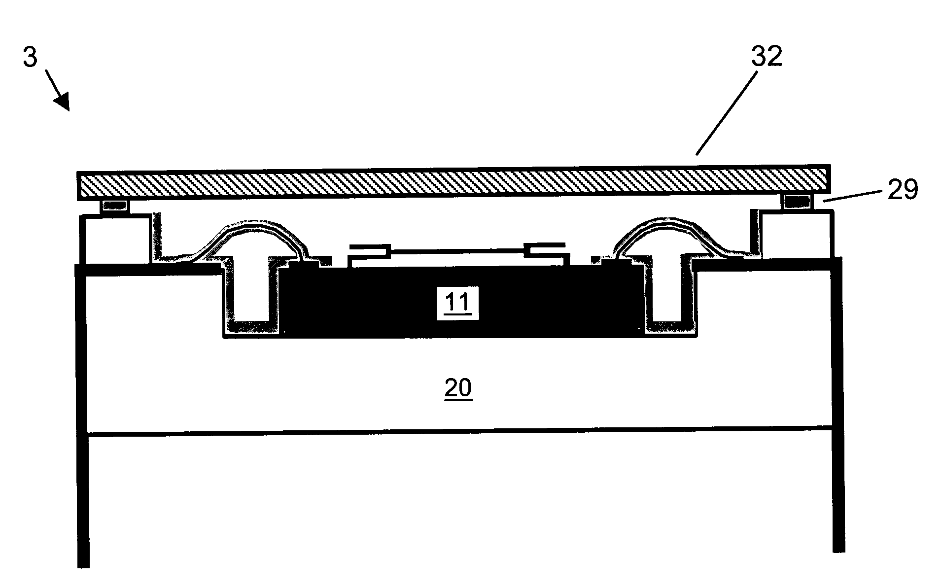
[0045]The present invention relates to methods to protect a MEMS or microsensor device through one or more release or activation steps in a “package first, release later” manufacturing scheme. This method of fabrication permits wirebonds, other interconnects, packaging materials, lines, bond pads, and other structures on the die to be protected from physical, chemical, or electrical damage during the release etch(es) or other packaging steps. Metallic structures (e.g., gold, aluminum, copper) on the device are also protected from galvanic attack because they are protected from contact with HF or HCL acid etch solutions.

Definitions

[0046]Herein, the word “wafer” is defined to include not only silicon, but also germanium, gallium arsenide (GaAs), other semiconducting materials, and also quartz wafers or substrates (e.g., for MEMS structures), and silicon on insulator (SOI). Substrates such as alumina, LTCC, HTCC, and polymer are also included. Use of the word “MEMS” is intended to also...


PUM

PropertyMeasurementUnit
Lengthaaaaaaaaaa
Thicknessaaaaaaaaaa
Electrical conductivityaaaaaaaaaa

Abstract

The present invention relates to methods to protect a MEMS or microsensor device through one or more release or activation steps in a “package first, release later” manufacturing scheme: This method of fabrication permits wirebonds, other interconnects, packaging materials, lines, bond pads, and other structures on the die to be protected from physical, chemical, or electrical damage during the release etch(es) or other packaging steps. Metallic structures (e.g., gold, aluminum, copper) on the device are also protected from galvanic attack because they are protected from contact with HF or HCL-bearing solutions.

Description

CROSS-REFERENCE TO RELATED APPLICATIONS[0001]This application is a continuation-in-part application of U.S. patent application Ser. No. 09 / 955,722, entitled “Temporary Coatings for Protection of Microelectronic Devices During Packaging”, to Kenneth A. Peterson et al., filed on Sep. 18, 2001, now U.S. Pat. No. 6,844,623 which was a division of U.S. patent application Ser. No. 09 / 572,562, filed May 16, 2000, now U.S. Pat. No. 6,335,224, “Protection of Microelectronic Devices During Packaging”, and the specifications thereof are incorporated herein by reference. This application claims the benefit of U.S. Provisional Application No. 60 / 438,028, “Encapsulants for Protecting MEMS Devices During Post-Packaging Release Etch”, filed Jan. 2, 2003, which is incorporated herein by reference.GOVERNMENT RIGHTS[0002]The Government has rights to this invention pursuant to Contract No. DE-AC04-94AL85000 awarded by the U.S. Department of Energy.BACKGROUND OF THE INVENTION[0003]The present invention ...

Claims


Application Information

Patent Timeline
IPC IPC(8): H01L23/48H01L23/02H01L23/34H01L23/40H01L23/52B81B7/00B81C1/00H01L21/56H01L23/31H01L23/49
CPCB81B7/0025B81C1/00333B81C1/00801H01L21/56H01L23/3121H01L24/16H01L24/48B81B2207/115B81C2201/053B81C2201/056H01L2224/05599H01L2224/13099H01L2224/16H01L2224/45124H01L2224/45144H01L2224/45147H01L2224/48091H01L2224/48227H01L2224/484H01L2224/48599H01L2224/48699H01L2224/49175H01L2224/85399H01L2224/8592H01L2924/01005H01L2924/01006H01L2924/01013H01L2924/01014H01L2924/01022H01L2924/01028H01L2924/01029H01L2924/01031H01L2924/01032H01L2924/01042H01L2924/0105H01L2924/01073H01L2924/01074H01L2924/01077H01L2924/01078H01L2924/01079H01L2924/01082H01L2924/01322H01L2924/014H01L2924/09701H01L2924/10329H01L2924/14H01L2924/15153H01L2924/15165H01L2924/19041H01L2924/19042H01L2924/19043H01L2924/3025H01L2924/00014H01L24/45H01L24/49H01L2924/01023H01L2924/01024H01L2924/01033H01L2924/01072H01L2924/06H01L2924/00H01L2224/48799H01L2224/0401H01L2224/04042H01L2924/10253H01L2224/16225H01L2224/85203H01L2224/16227H01L2224/8192H01L2924/181H01L2224/05554H01L2924/16195
Inventor PETERSON, KENNETH A.
Owner NAT TECH & ENG SOLUTIONS OF SANDIA LLC
Why Eureka
Try Eureka