
Patterning method for fabricating integrated circuit

Active Publication Date: 2005-09-20
MACRONIX INT CO LTD
View PDF3 Cites 16 Cited by
  • Summary
  • Abstract
  • Description
  • Claims
  • Application Information

AI Technical Summary

Benefits of technology

[0008]Accordingly, one object of the present invention is to provide a patterning method for fabricating integrated circuits that can relax some of the limitations in a photolithographic process.
[0009]A second object of this invention is to provide a patterning method for fabricating integrated circuits that resolves some of the drawbacks caused by using a hard mask layer in the conventional method.
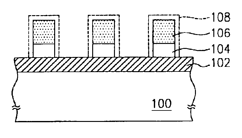
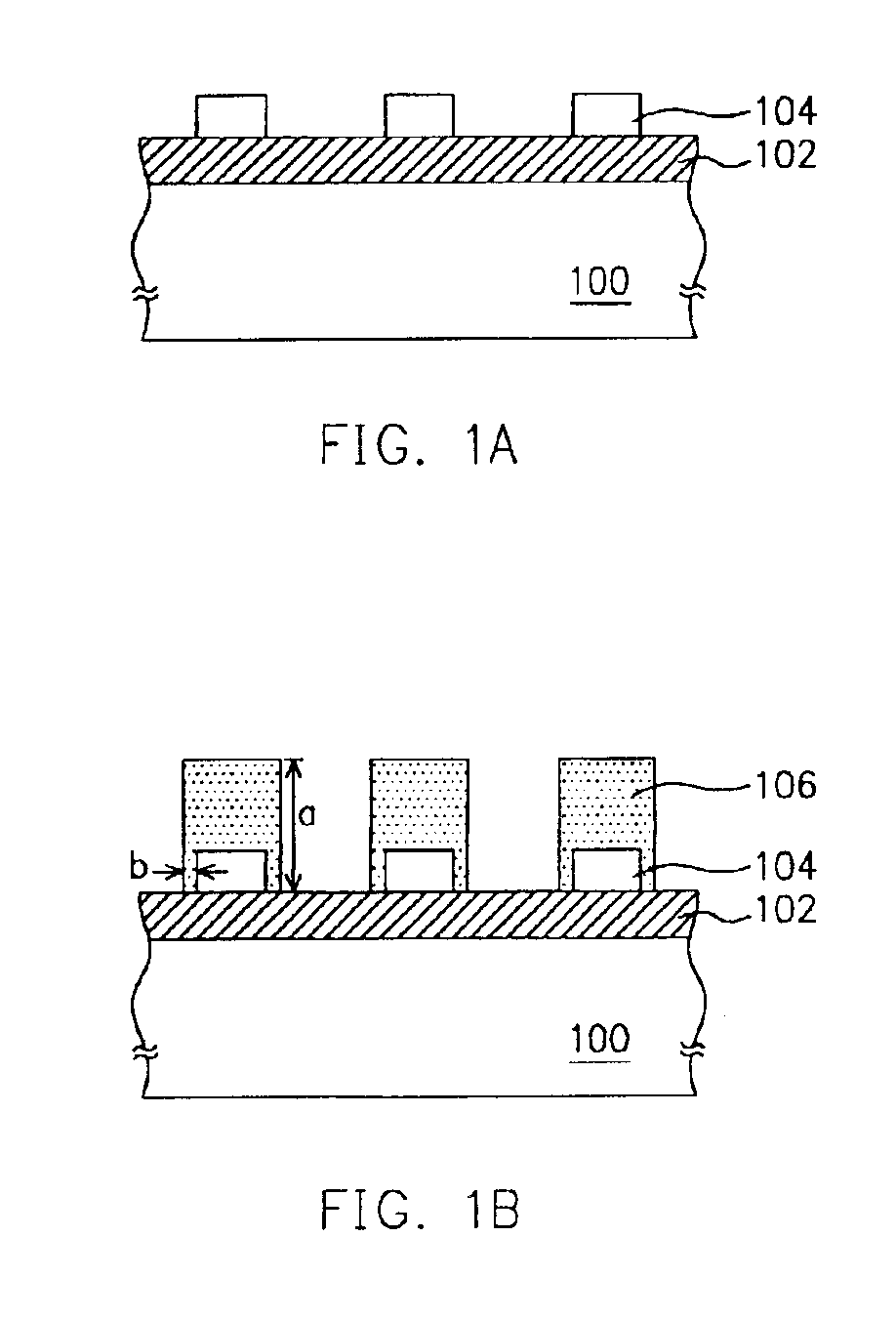
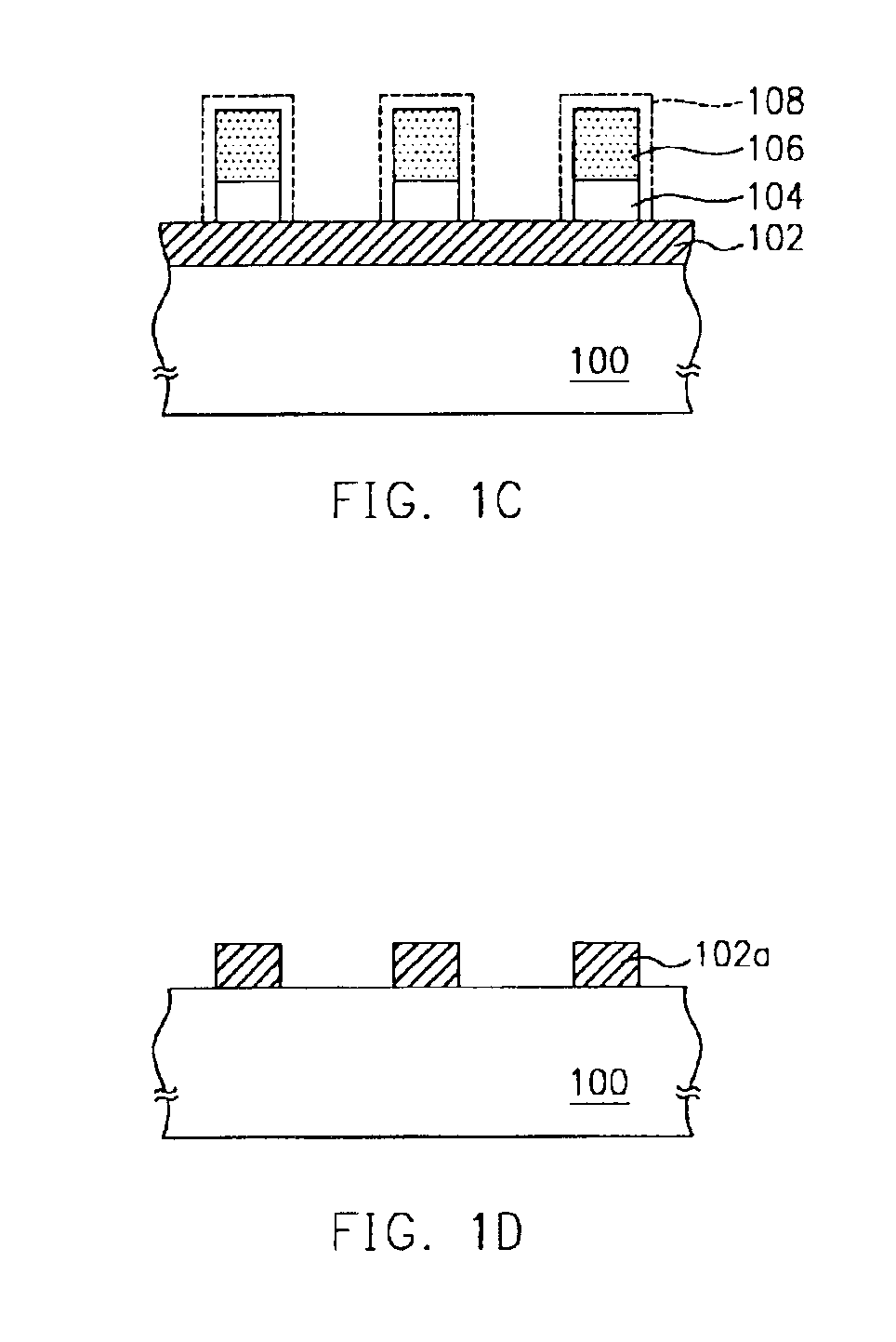
[0012]In this invention, a thinner photoresist layer is fabricated so that the limitations in photolithographic process due to device miniaturization are eased. Although the photoresist layer is too thin to resist etching, the shroud liner rather than the photoresist layer actually serves as as etching mask. Hence, the method is able to relax the limitations in a photolithographic process and to miniaturize devices at the same time.

Problems solved by technology

Furthermore, if the mask is used as an etching mask, gap or opening dimension in the etching mask can hardly be reduced without some adverse effect on the underlying layer waiting to be etched.
Hence, miniaturization of device can hardly be achieved by reducing thickness of the photoresist layer directly.
Yet, this method has some serious drawbacks.
Hence, a different hard mask layer must be used to pattern a material layer made from a different material and hence the complexity of processing design is increased.
Secondly, because the hard mask layer and the photoresist layer must be made from two different materials, the photoresist layer and the hard mask layer must be removed in at least two separate steps and hence the complexity the fabrication is more complex and, thus, more costly.

Method used


Image

  • Patterning method for fabricating integrated circuit
  • Patterning method for fabricating integrated circuit
  • Patterning method for fabricating integrated circuit

Examples


first embodiment

[0028]In this embodiment, the shroud liner 206 is, for example, a polymeric material. The shroud liner 206 is formed, for example, by plasma-enhanced chemical vapor deposition (PECVD). In the PECVD, reactive gases having a chemical formula CxFy and CHmFn (where x, y, m, n are integers) are used. Since a process of using PECVD to form a shroud liner as in the first embodiment is used, a detailed description is not repeated here.

[0029]Thereafter, using the trimmed shroud liner 206 as etching mask, etching is conducted to pattern the material layer 202 into a material layer 202a. Finally, the shroud liner 206 and the photoresist layer 204 are removed to produce the structure as shown in FIG. 2C. Since the shroud liner 206 and the photoresist layer 204 are made from similar organic polymer is material, the shroud liner 206 and the photoresist layer 204 can be removed together in a single step.

second embodiment

[0030]In the aforementioned second embodiment, the photoresist layer 204 is purposely made thinner to relax the limitations in a photolithographic process resulting from patterning a thick photoresist layer 204. Although the photoresist layer 204 is too thin to resist subsequent etching, the shroud liner 206 rather than the photoresist layer 204 is actually used as etching mask for patterning the material layer 202. Hence, the invention is able to relax some of the limitations in photolithographic and etching process as and to enable reducing device dimensions accordingly. In addition, width of the shroud liner 206 is also purposely made to match the critical dimension “c” of a device. Since the critical dimensions of a semiconductor device are very important in the fabrication of semiconductor, a number of methods for controlling critical dimension have been developed. In this invention, critical dimension of the device is controlled by the growth of the shroud liner 206. The metho...


PUM


Abstract

A patterning method for fabricating integrated circuits. The method includes forming a material layer over a substrate and then forming a photoresist layer over the material layer. The photoresist layer has a thickness small enough to relax the limitations when the photoresist layer is patterned in a photolithographic process. A shroud liner is formed over the photoresist layer such that height of the shroud liner is significantly greater than width of the shroud liner. Thereafter, the shroud liner undergoes a processing treatment to remove the sections attached to the sidewalls of the photoresist layer. Using the remaining shroud liner as an etching mask, an etching operation is carried out to pattern the material layer.

Description

CROSS REFERENCE TO RELATED APPLICATIONS[0001]This application claims the priority benefit of Taiwan application serial no. 91137112, filed Dec. 24, 2002.BACKGROUND OF INVENTION[0002]1. Field of Invention[0003]The present invention relates to a patterning method for fabricating integrated circuit. More particularly, the present invention relates to a patterning method capable of minimizing some limitations in photolithographic and etching processes.[0004]2. Description of Related Art[0005]As dimensions of semiconductor devices continue to shrink, the demand for resolution goes up correspondingly. Because the resolution of a photolithographic process is dependent upon wavelength of a light source used in the photo-exposure, the mask patterns obtained by conducting a photolithographic (or together with an etching) process must be separated from each other by a minimum distance. Furthermore, if the mask is used as an etching mask, gap or opening dimension in the etching mask can hardly ...

Claims


Application Information

Patent Timeline
IPC IPC(8): H01L21/02H01L21/027H01L21/3213H01L21/311H01L21/033
CPCH01L21/0271H01L21/0273H01L21/32139H01L21/31144H01L21/0338H01L21/0337
Inventor CHUNG, HENRY
Owner MACRONIX INT CO LTD
Learn More