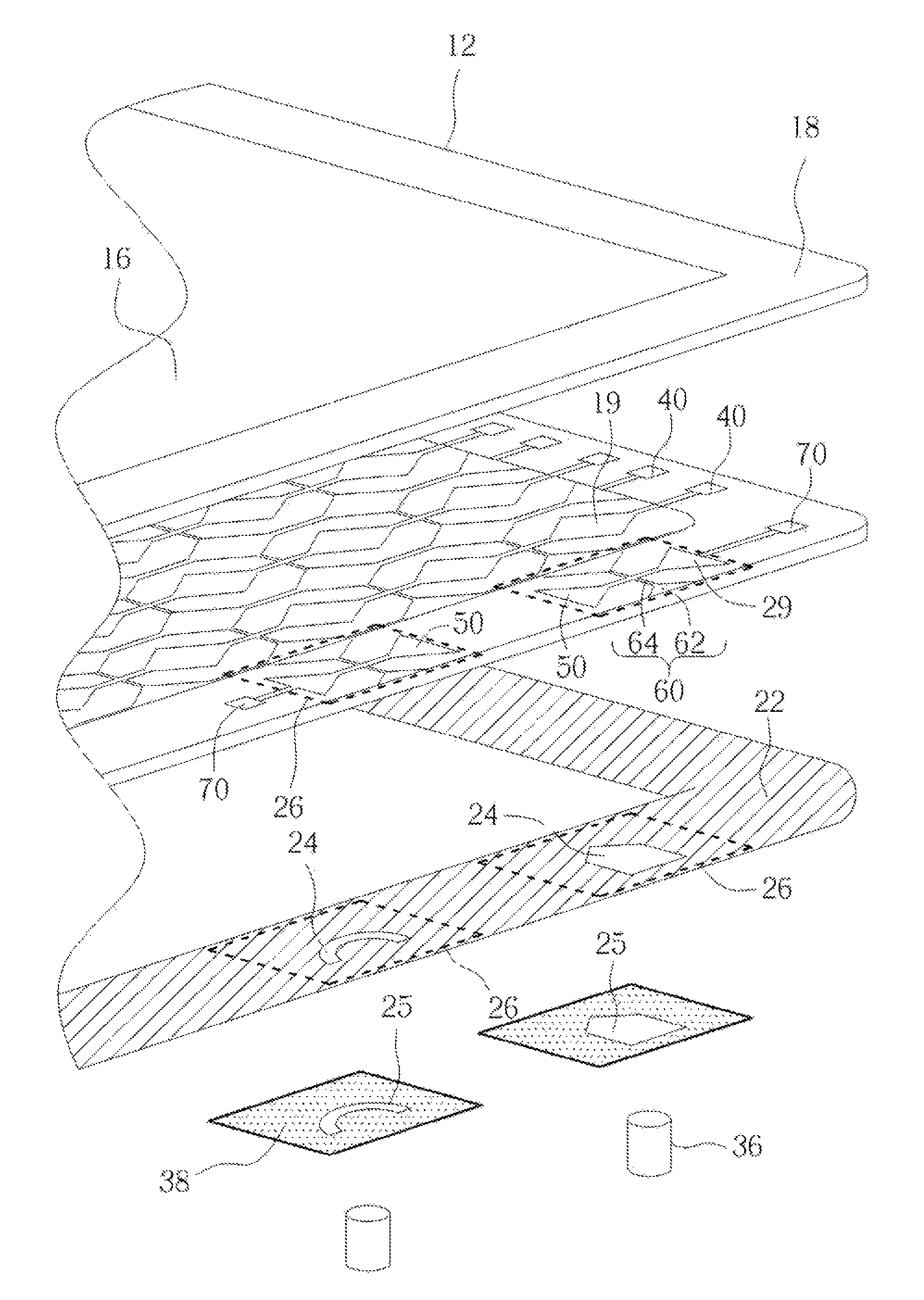
Touch panel
a touch panel and touch technology, applied in the field of touch technology, can solve the problems of affecting the appearance of products, pinholes formed in the shelter layer, and the space allowed in these new-developed electronic products is no longer enough to accommodate conventional input devices such as key boards or mice, so as to improve the appearance of products
- Summary
- Abstract
- Description
- Claims
- Application Information
AI Technical Summary
Benefits of technology
Problems solved by technology
Method used
Image
Examples
first embodiment
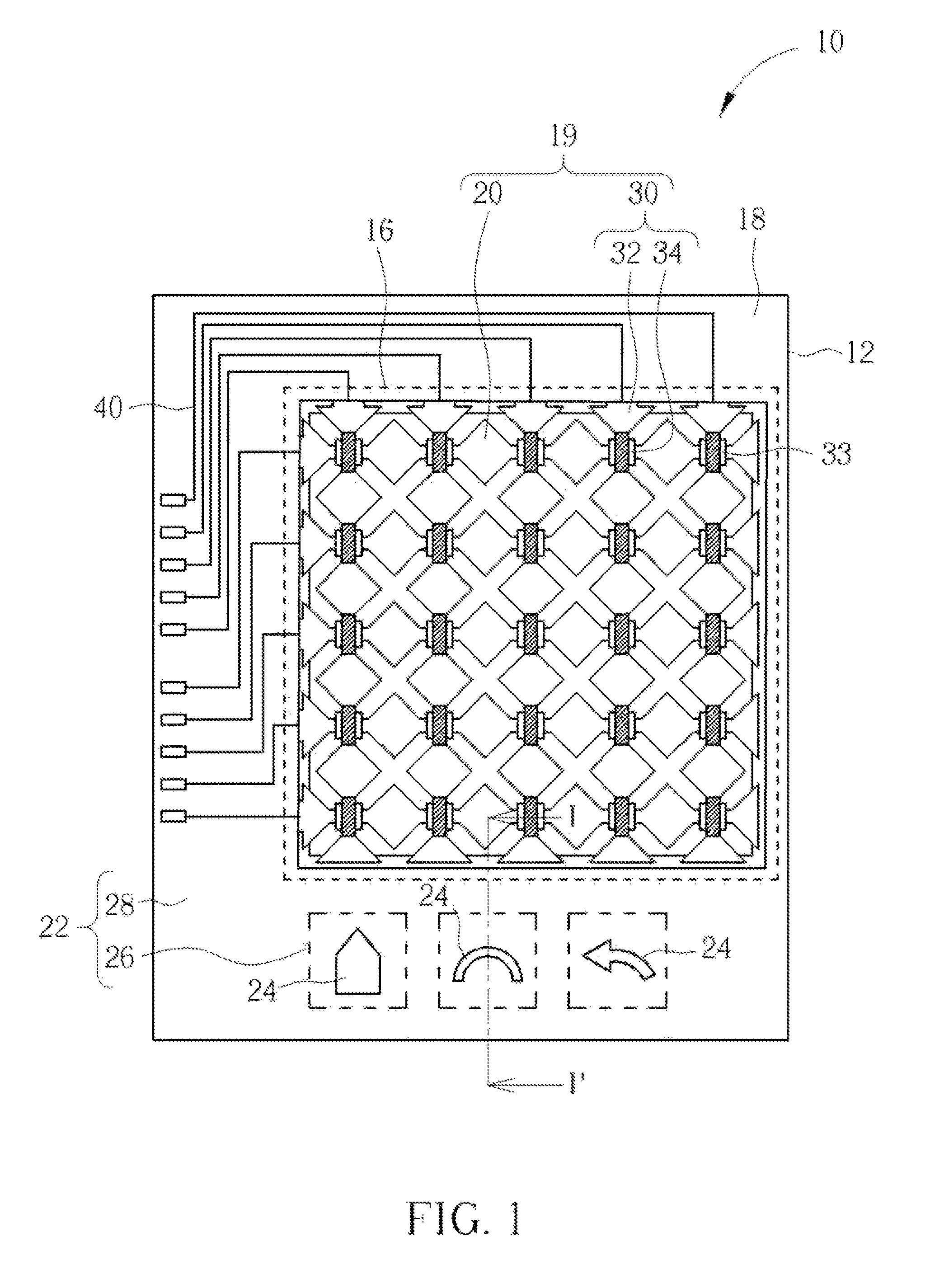
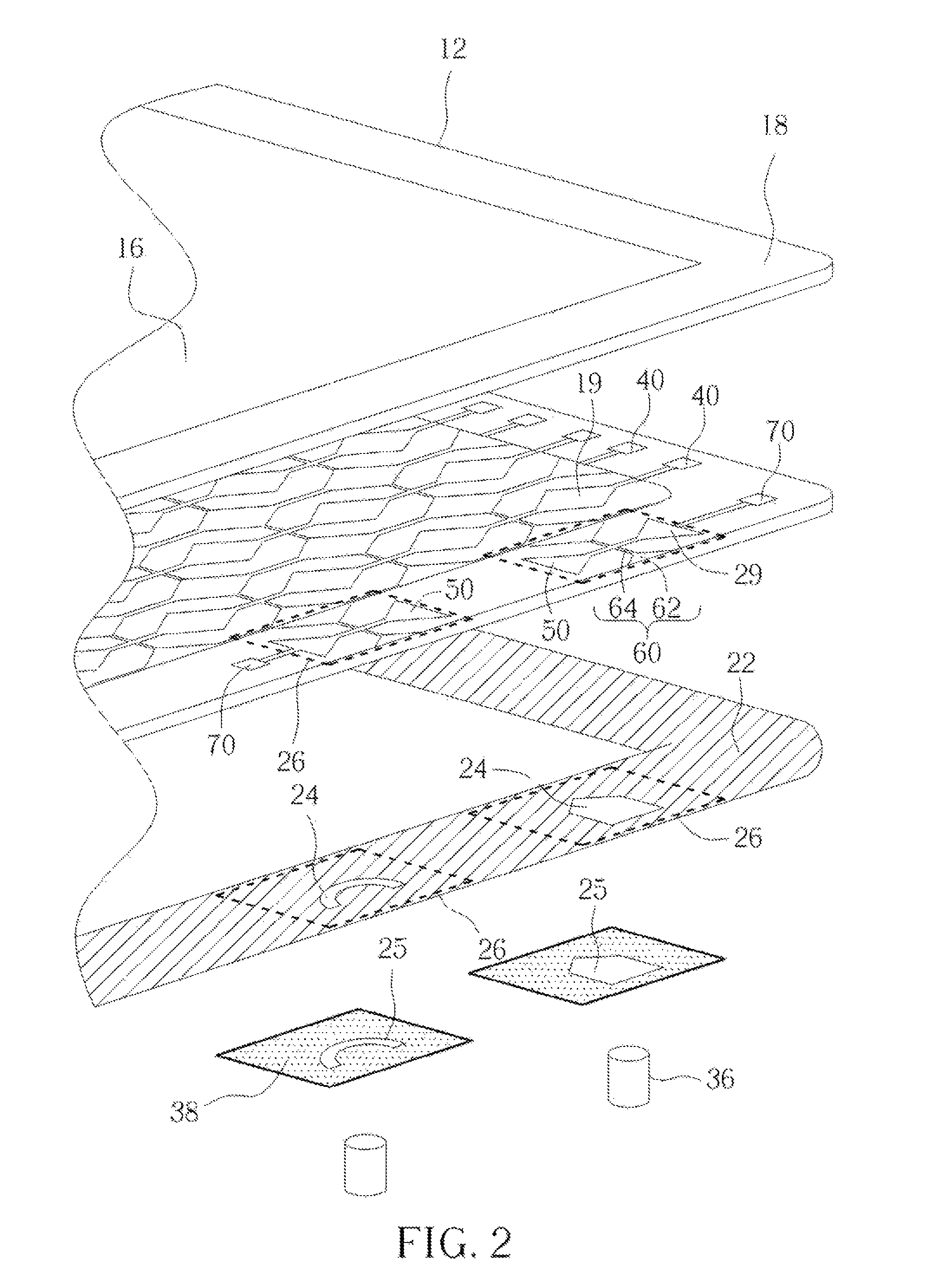
[0021]FIG. 1 is a schematic, top-view showing a touch panel according to the present invention. Referring to FIG. 1, a touch panel 10 disclosed in the present invention includes a protective cover 12, such as a reinforced cover glass. An active region 16 and a peripheral region 18 surrounding the active region 16 are defined on the protective cover 12. A first sensing structure 19 is disposed on a lower surface of the protective cover 12 and covers the active region 16. In this embodiment, the first sensing structure 19 includes a plurality of parallel first axis electrodes 20 extending along a first direction (i.e. X-axis in this embodiment), and a plurality of parallel second axis electrodes 30 extending along a second direction (i.e. Y-axis in this embodiment). In addition, each of the second axis electrodes 30 includes a plurality of conductive units 32 and at least a connection line 34 used to electrically connect two adjacent conductive units 32. An isolation layer 33 is dispo...
fourth embodiment
[0030]In the above-mentioned embodiments, the first sensing structure 19 and the second sensing structure 29 are directly formed on the protective cover 12. This structure, without any substrate to support the first sensing structure 19 and the second sensing structure 29, is also called Touch On Lens (TOL) structure. According to another embodiment, however, a touch panel of the present invention may also have another substrate in order to support the first sensing structure 19 and the second sensing structure 29. FIG. 6 is a schematic, cross-sectional diagram showing a touch panel according to a fourth preferred embodiment of the present invention. Referring to FIG. 6, a touch panel according to the fourth preferred embodiment includes a substrate 42 and a protective cover 12. An active region 16 and a peripheral region 18 are defined on the protective cover 12. A shelter layer 22 is formed on the protective cover 12 corresponding to the peripheral region 18. At least a highlight ...
seventh embodiment
[0033]FIG. 9 is a schematic, cross-sectional diagram showing a touch panel according to a seventh preferred embodiment of the present invention. One difference between the fourth preferred embodiment and the seventh preferred embodiment is that the substrate 42 and the second sensing structure 29, are disposed between the shelter layer 22 and the non transparent layer 38. The rest of the parts disclosed in this embodiment, as well as the characteristics of other parts, material properties and the way of fabricating are almost similar to those described in the first preferred embodiment. For the sake of brevity, these similar configurations and properties are therefore not disclosed again in detail.
[0034]FIG. 10 is a schematic, cross-sectional diagram showing a touch panel according to an eighth preferred embodiment of the present invention. One difference between the fourth preferred embodiment and the eighth preferred embodiment is that the substrate 42 and the second sensing stru...
PUM
 Abstract
Description
Claims
Application Information
 - R&D
- Intellectual Property
- Life Sciences
- Materials
- Tech Scout
- Unparalleled Data Quality
- Higher Quality Content
- 60% Fewer Hallucinations
Browse by: Latest US Patents, China's latest patents, Technical Efficacy Thesaurus, Application Domain, Technology Topic, Popular Technical Reports.
© 2025 PatSnap. All rights reserved.Legal|Privacy policy|Modern Slavery Act Transparency Statement|Sitemap|About US| Contact US: help@patsnap.com


