Clock gated power supply noise compensation

a power supply and noise compensation technology, applied in the field of integrated circuit design systems, can solve the problems of timing uncertainty, random entry of latch metastability, invalid latch data, etc., and achieve the effect of minimizing how it affects circuit performan

Inactive Publication Date: 2005-08-23
IBM CORP
View PDF13 Cites 24 Cited by
  • Summary
  • Abstract
  • Description
  • Claims
  • Application Information

AI Technical Summary

Benefits of technology

[0010]It is another purpose of the invention to reduce dI / dt chip effects;
[0012]It is yet another purpose of the invention to sense the onset of dI / dt noise and take steps to minimize how it affects circuit performance.

Problems solved by technology

Unfortunately, various chip differences can cause timing uncertainty, i.e., a variation in edge arrival to different registers.
Such timing uncertainties can arise from data propagation variations and / or from clock arrival variations.
Data propagation variations, for example, may result in a capturing latch that randomly enters metastability or latches invalid data because the data may or may not arrive at its input with sufficient set up time.
In particular, power supply noise can cause clock propagation delay variations through clock distribution buffers.
Such clock propagation delay variations can cause skew variations from clock edge arrival time uncertainty at the registers.
Especially for clock distribution buffers, these process variations are another source of timing uncertainty.
Furthermore, as technology features continue to shrink, power bus or Vdd noise is becoming the dominant contributor to total timing uncertainty.
High speed circuit switching may cause large, narrow current spikes with very rapid rise and fall times, i.e., large dI / dt.
In particular, each of those current spikes cause substantial voltage spikes in the on-chip supply voltage, even when power supply inductance (L) is minimized.
Since current switching can vary from cycle to cycle, the resulting noise varies from cycle to cycle.
When the Vdd noise drops the on-chip supply voltage in response to a large switching event, it slows the entire chip, including both the clock path (clock buffers, local clock blocks, clock gating logic and etc.) as well as the data path logic (combinational logic gates, inverters and etc.) and may cause the chip to fail.
If the supply rises too far above nominal, devices may be stressed beyond breaking to damage the chip or, at the very least reduce chip reliability.
Currently, in particular, such switching noise is a significant component of total timing uncertainty, comparable to skew or jitter (which are themselves affected by switching noise) or chip process variations.

Method used


Image

  • Clock gated power supply noise compensation
  • Clock gated power supply noise compensation
  • Clock gated power supply noise compensation

Examples


Embodiment Construction

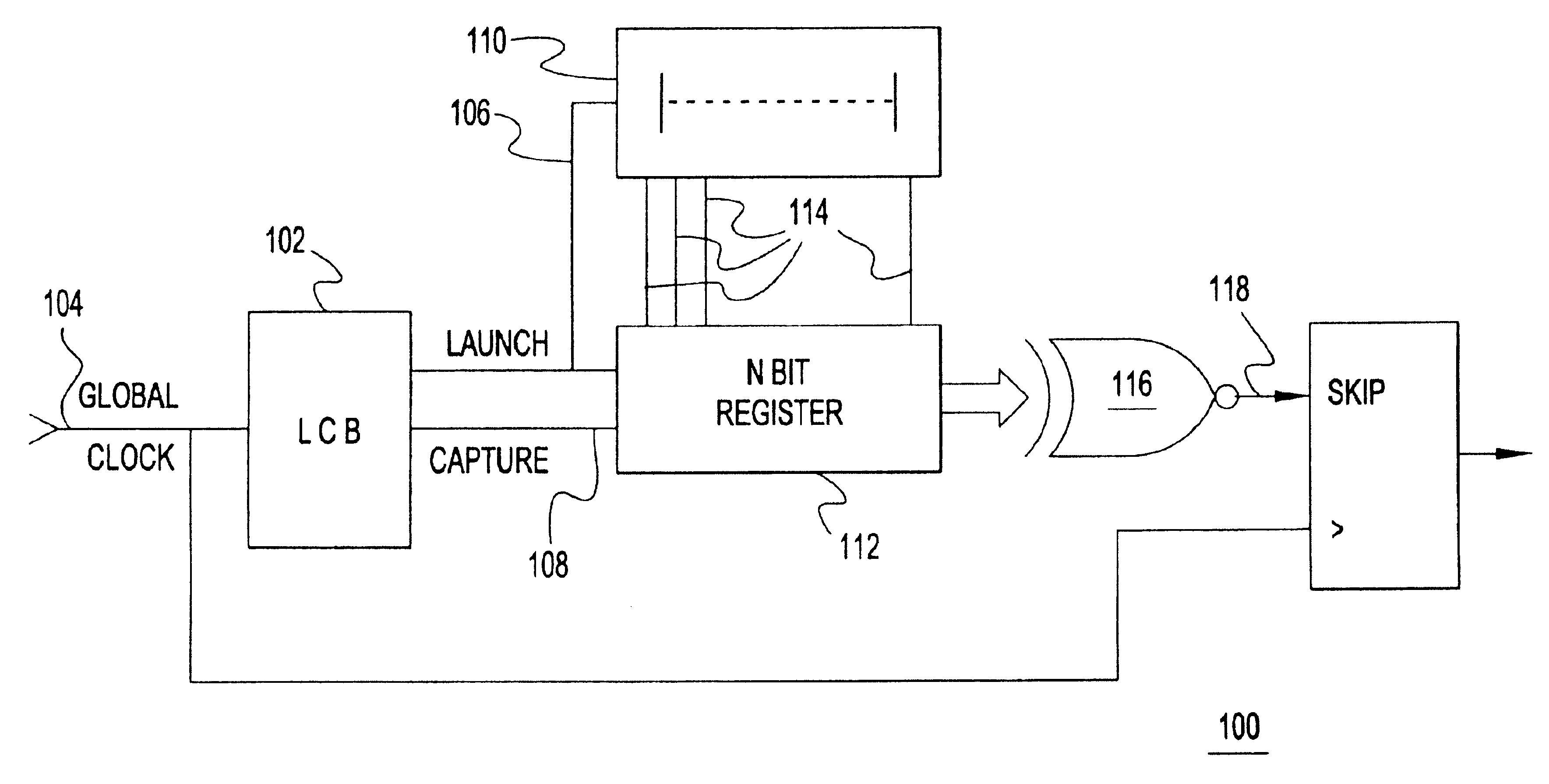
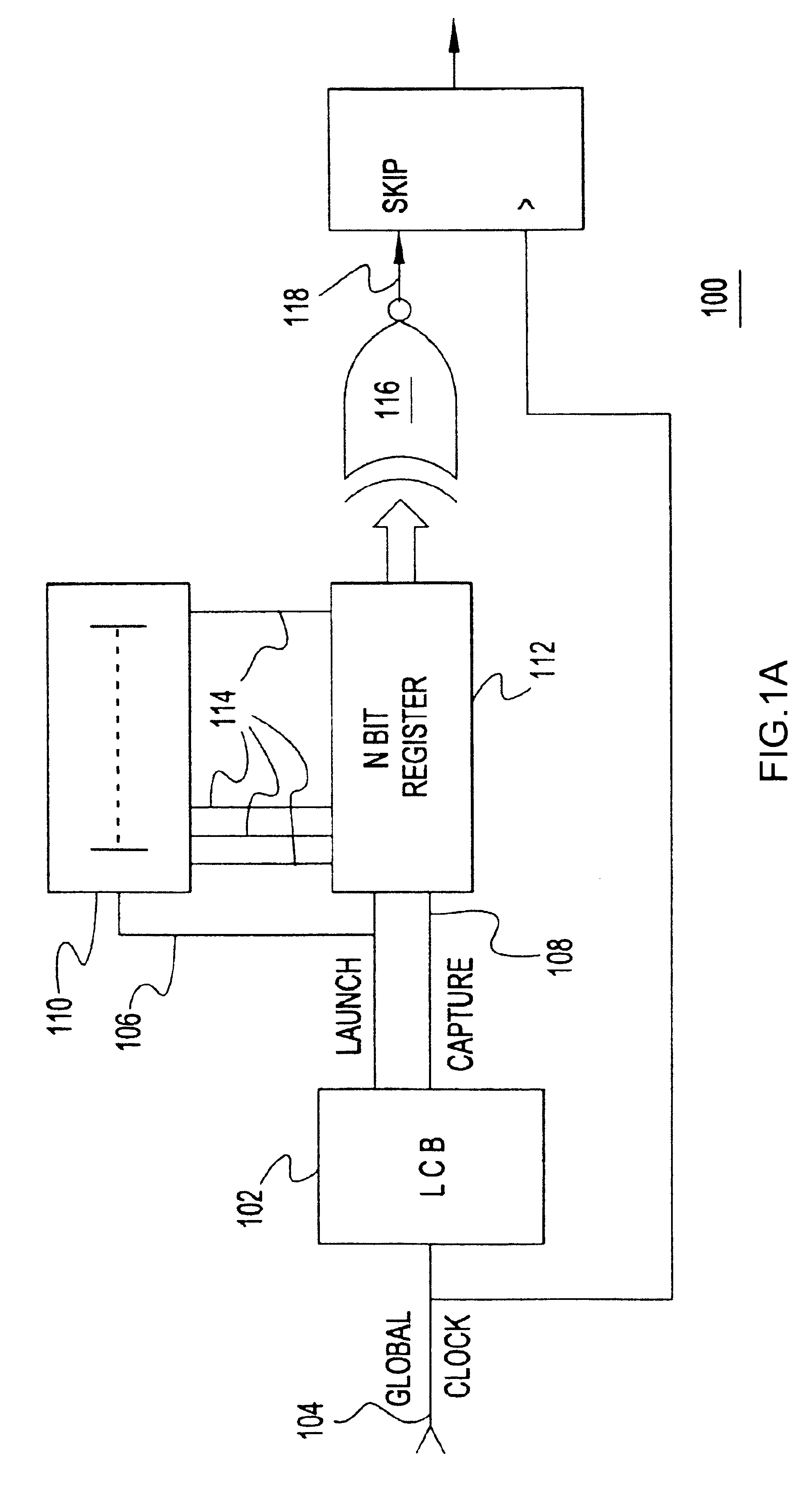
[0018]Turning now to the drawings and, more particularly, FIGS. 1A-C show block diagram examples of a supply noise compensation circuit 100 according to a preferred embodiment of the present invention. A local clock block (LCB) or clock buffer 102 receives and re-drives a global chip clock 104 into 2 complementary local clocks 106, 108. One clock, a launch clock 106, is provided as an input to a delay line 110 that is sensitive to supply voltage changes. The local clock, e.g., launch clock 106, enters the delay line 110 and, as it propagates through the delay line 110, the LCB 102 and delay line 110 mimic data propagation delay through an actual data path, e.g., in a microprocessor 122. In particular, the launch clock propagating along the delay line 110 reflects propagation delay variations resulting from switching or dI / dt noise on the Circuit power supply (Vdd) line. Both the launch clock 106 and the second clock, a capture clock 108, clock an N bit register 112. For example, N=1...


PUM


Abstract

A supply noise compensation circuit. The supply noise compensation circuit senses the onset of dI / dt noise events on a supply line and selectively gates off / forces on a chip clock to chip circuits.

Description

CROSS REFERENCE TO RELATED APPLICATION[0001]The present invention is related to U.S. application Ser. No. 10 / 712,925 entitled “BUILT IN SELF TEST FOR MEASURING TOTAL TIMING UNCERTAINTY IN A DIGITAL DATA PATH” to Robert L. Franch et al., filed coincident herewith and assigned to the assignee of the present invention.BACKGROUND OF THE INVENTION[0002]1. Field of the Invention[0003]The present invention is related to integrated circuit (IC) design systems and more particularly to characterizing timing uncertainties in ICs.[0004]2. Background Description[0005]Large high performance very large scale integration (VLSI) chips like microprocessors are synchronized to an internal clock. A typical internal clock is distributed throughout the chip, triggering chip registers to synchronously capture incoming data at the register latches and launch data from register latches. Ideally, each clock edge arrives simultaneously at each register every cycle and data arrives at the register latches suff...

Claims


Application Information

Patent Timeline
Patent Type & Authority Patents(United States)
IPC IPC(8): H03L5/00H03L7/00H03K5/153G06F1/10H03K5/1252
CPCG06F1/10H03K5/1252
Inventor RESTLE, PHILLIP J.
Owner IBM CORP
Why Eureka
Try Eureka