
Ultra high-speed Si/SiGe modulation-doped field effect transistors on ultra thin SOI/SGOI substrate

a field effect transistor and high-speed technology, applied in semiconductor devices, semiconductor/solid-state device details, electrical apparatus, etc., can solve the problems of reducing drive current and self-heating, and achieve high rf performan

Active Publication Date: 2005-02-15
GLOBALFOUNDRIES US INC
View PDF1 Cites 25 Cited by
  • Summary
  • Abstract
  • Description
  • Claims
  • Application Information

AI Technical Summary

Benefits of technology

The invention is directed to a high-electron-mobility n-channel MODFET device that is properly scaled and constructed on a thin SGOI / SOI substrate that exhibits greatly improved RF performance.
The present invention is directed to a MODFET device and method of manufacture that addresses the prior art limitations and achieves vertical scaling of the nMODFET layer structure and the source / drain junction and lateral scaling of the device structure to unprecedented degrees, resulting in a device exhibiting ultra-high speed performance (i.e. fT, fmax >300 GHz) with acceptable voltage gain and good turn-off characteristics.
In the method of manufacturing the MODFET device of the invention, the MODFET device is built on an ultra-thin SiGe-on-insulator (SGOI) substrate, such that the body is fully depleted. Due to the suppressed short channel effects, the output conductance (gd) may be thus be reduced. Therefore, the DC voltage gain (gm / gd), the linearity and fmax is significantly improved. In addition, the provision of ultra-thin SiGe buffer layers also reduces the self-heating due to the low thermal conductivity of SiGe, which reduces the drive current. Compared to a bulk MODFET, a fully-depleted SGOI MODFET exhibits better noise figures and lower soft error rate. Preferably, the epitaxial field effect transistor structure of the invention includes the critical device scaling and layer structure design for a high mobility strained n-channel transistor incorporating silicon and silicon germanium layers to form the optimum modulation-doped heterostructure on an ultra thin SOI or SGOI substrate in order to achieve fmax of >300 GHz.
The invention further is directed to a high-hole-mobility p-channel MODFET that is properly scaled and constructed on a thin SGOI / SOI substrate will also have very high RF performance.

Problems solved by technology

In addition, the provision of ultra-thin SiGe buffer layers also reduces the self-heating due to the low thermal conductivity of SiGe, which reduces the drive current.

Method used


Image

  • Ultra high-speed Si/SiGe modulation-doped field effect transistors on ultra thin SOI/SGOI substrate
  • Ultra high-speed Si/SiGe modulation-doped field effect transistors on ultra thin SOI/SGOI substrate
  • Ultra high-speed Si/SiGe modulation-doped field effect transistors on ultra thin SOI/SGOI substrate

Examples


first embodiment

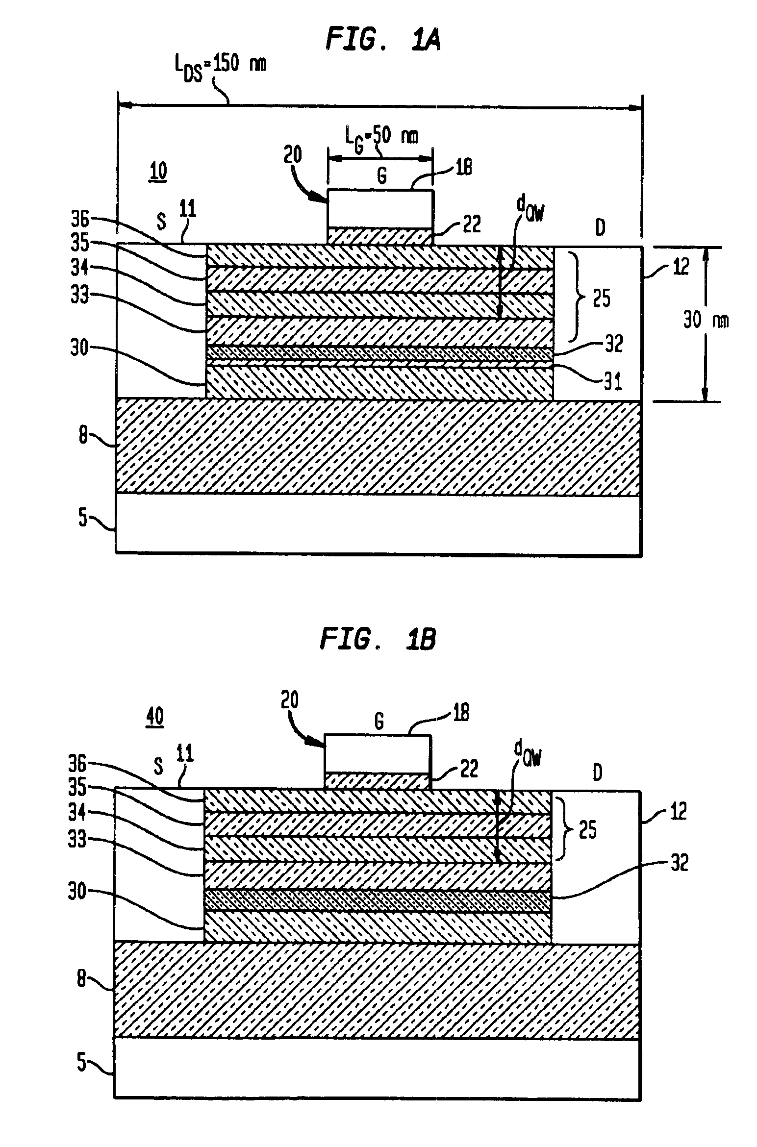
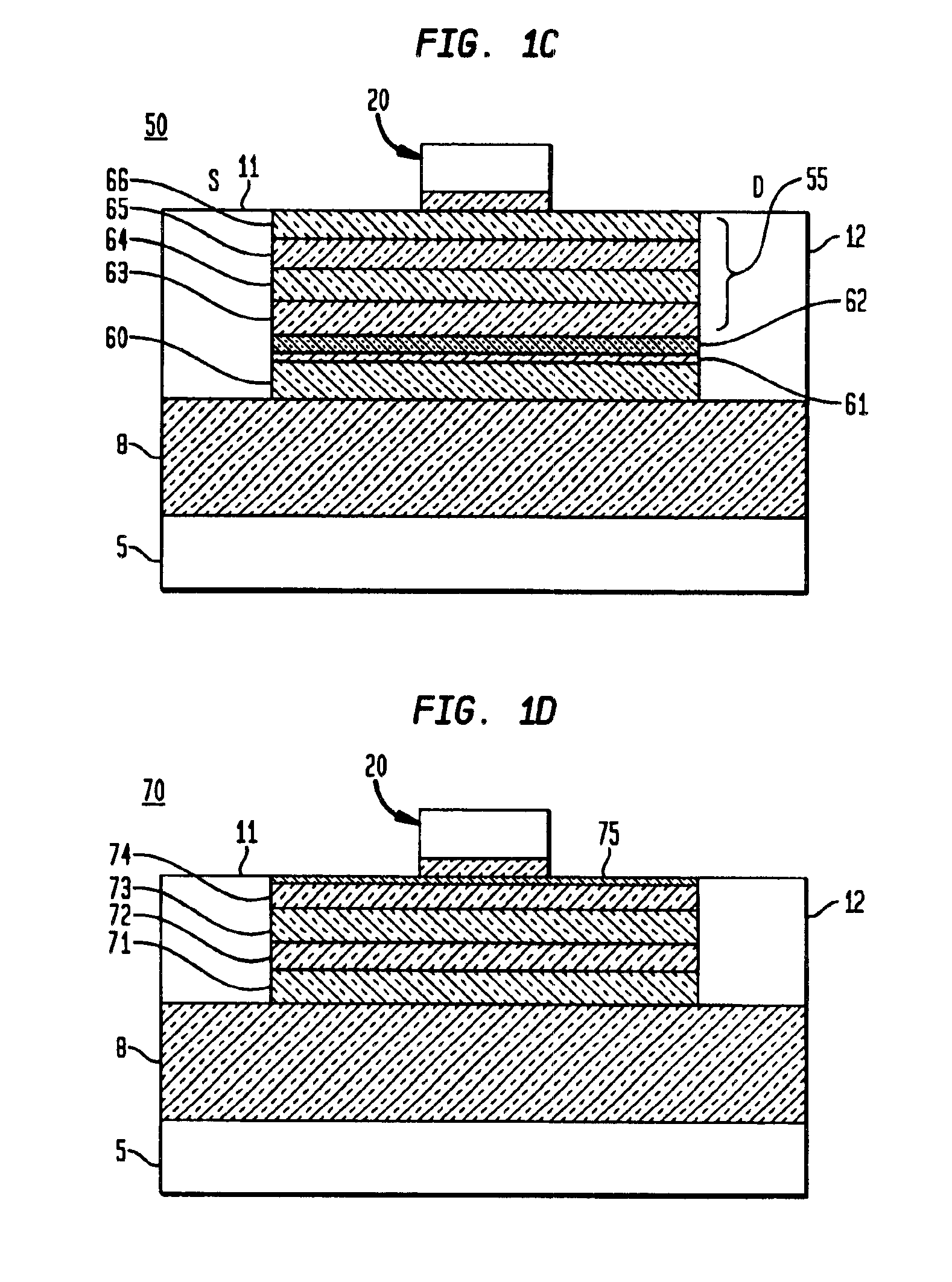
FIG. 1(a) particularly depicts a MODFET device according to a As shown in FIG. 1(a), there is depicted a top doped nMODFET device 10 comprising a Si substrate layer 5, a buried dielectric layer8 formed on top of the substrate 5 which may range up to 200 nm in thickness and comprise an oxide, nitride, oxynitride of silicon; and a channel region 25 formed between n+-type doped source and drain regions 11, 12 respectively, and a gate structure 20 including a gate dielectric layer 22 separating the gate conductor 18 from the channel 25. As shown in the figure, the gate dielectric layer may comprise an oxide, nitride, oxynitride of silicon, and oxides and silicates of Hf, Al, Zr, La, Y, Ta, singly or in combinations. It is important to realize that according to the invention, the dimensions of the device including drain, source, gate and channel regions have been scaled.

The composition of the channel region 25 of device 10 in FIG. 1(a) is as follows: A relaxed SiGe layer 30 having a p-t...

fifth embodiment

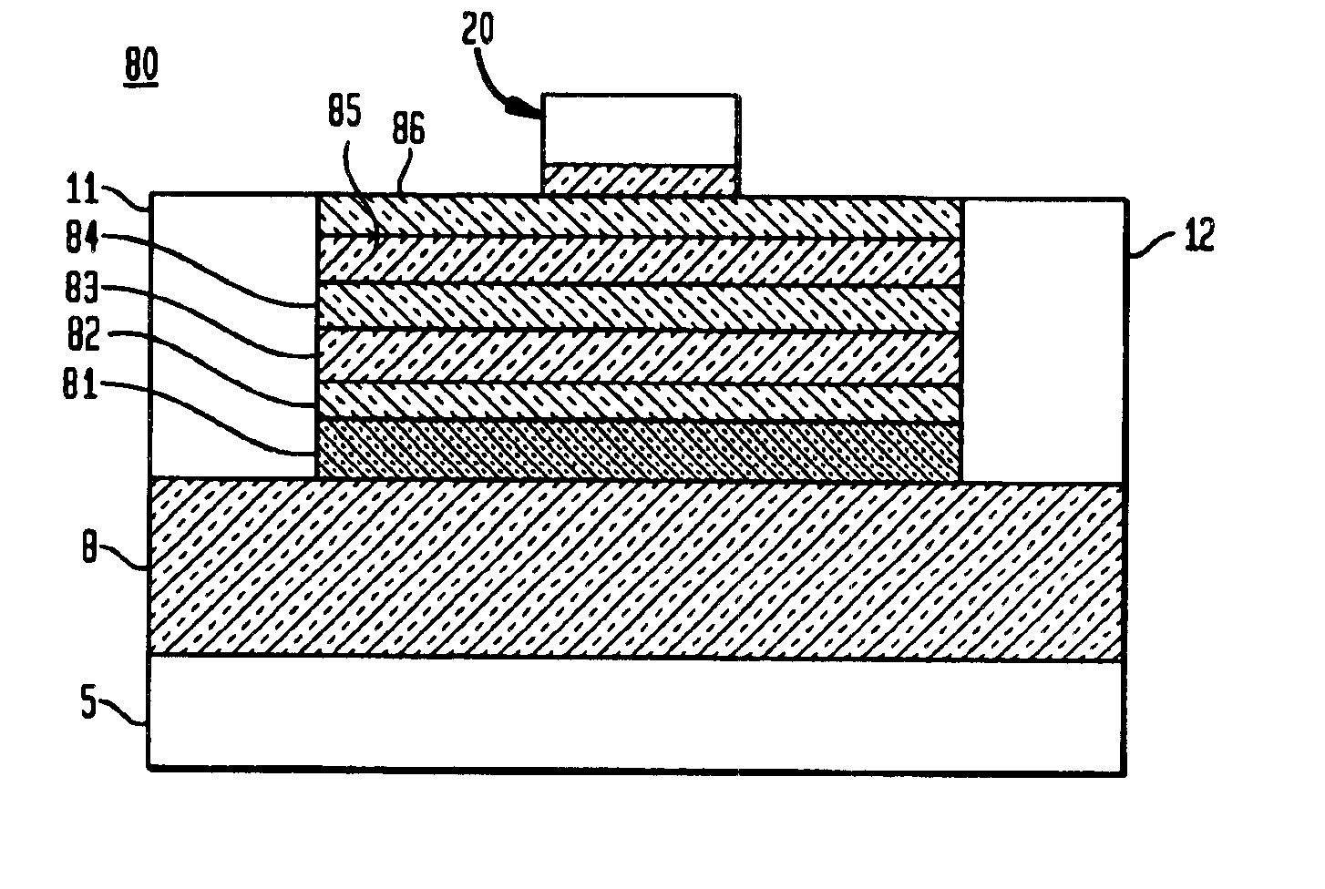
FIG. 1(f) illustrates the invention drawn to a high-hole-mobility MODFET device 80 that is bottom doped and including a doped transferred layer. As shown in FIG. 1(f), the pMODFET device 90 includes an SGOI (SiGe layer 91 on insulator 8) substrate having: a relaxed epitaxial Si1-jGej supply layer ranging in thickness between 5 nm-25 nm, and having ion-implanted or in-situ p-type doping of a concentration ranging between 1e18-5e19 cm−3 and serving as a supply layer. Alternately, the relaxed Si1-jGej layer may be predoped p-type to a concentration level of 1e18-5e19 boron atoms / cm3 before a layer transfer in forming the SGOI substrate; an epitaxial Si1-kGek spacer layer 92 grown on top of the supply layer 91 and ranging in thickness between 3 nm-7 nm; an epitaxial compressively strained Si1-mGem channel layer 93 grown on top of the spacer layer and ranging in thickness between 5 nm-20 nm; and, an epitaxial strained Si1-nGen cap layer 94 grown on top of the strained Si1-mGem channel la...


PUM


Abstract

A silicon and silicon germanium based semiconductor MODFET device design and method of manufacture. The MODFET design includes a high-mobility layer structure capable of ultra high-speed, low-noise for a variety of communication applications including RF, microwave, sub-millimeter-wave and millimeter-wave. The epitaxial field effect transistor layer structure includes critical (vertical and lateral) device scaling and layer structure design for a high mobility strained n-channel and p-channel transistor incorporating silicon and silicon germanium layers to form the optimum modulation-doped heterostructure on an ultra thin SOI or SGOI substrate capable of achieving greatly improved RF performance.

Description

BACKGROUND OF THE INVENTION1. Field of the InventionThe present invention relates generally to silicon and silicon germanium based semiconductor transistor devices, and more specifically, to a device design including a grown epitaxial field effect transistor structure capable of ultra high-speed, low-noise for a variety of communication applications including RF, microwave, sub-millimeter-wave and millimeter-wave. Preferably, the epitaxial field effect transistor structure includes the critical device scaling and layer structure design for a high mobility strained n-channel transistor incorporating silicon and silicon germanium layers to form the optimum modulation-doped heterostructure on an ultra thin SOI or SGOI substrate in order to achieve fmax in excess of 200 GHz.2. Description of the Prior ArtThe attractiveness of substantial electron mobility enhancement (i.e. 3-5 times over bulk silicon) in modulation-doped tensile-strained Si quantum wells has inspired a long history of d...

Claims


Application Information

Patent Timeline
IPC IPC(8): H01L21/02H01L29/786H01L29/10H01L29/02H01L29/778H01L29/66H01L21/335
CPCH01L29/78687H01L29/1054H01L21/18
Inventor CHU, JACK O.OUYANG, QIQING C.
Owner GLOBALFOUNDRIES US INC
Learn More