
Method for fabricating complementary metal oxide semiconductor (CMOS) devices on a mixed bulk and silicon-on-insulator (SOI) substrate

a technology of complementary metal oxide semiconductor and soi substrate, which is applied in semiconductor/solid-state device manufacturing, basic electric elements, electric devices, etc., can solve the problems of trench capacitor dram devices, which are typically built on bulk silicon substrates, and cannot be easily built on soi substrates

Inactive Publication Date: 2001-04-10
GLOBALFOUNDRIES INC
View PDF12 Cites 73 Cited by
  • Summary
  • Abstract
  • Description
  • Claims
  • Application Information

AI Technical Summary

Benefits of technology

In a first aspect of the present invention, a method of forming a semiconductor device, includes patterning a groove into a bulk silicon substrate, forming an oxide in said groove and planarizing the silicon substrate to form at least one patterned oxide island in the silicon substrate, forming a silicon layer on exposed portions of the silicon substrate and the at least one oxide island, crystallizing the silicon layer using the exposed silicon substrate as a seed, the silicon substrate having direct contact with the formed silicon layer serving as a crystal growth seeding for the crystallization process, and converting the silicon layer to crystallized silicon, performing a shallow trench isolation (STI) process for device isolation as well as for removing defective regions after silicon crystallization to form the oxide isolations between devices, wherein a portion of the silicon layer above the islands is etched to form a cavity and then the same material as the islands is deposited in the cavity, and planarizing the upper surface to complete the oxide isolations. It is noted that an advantage of the present invention is that by performing the STI process also simultaneously removes the defective regions by filling the same with oxide.
With the unique and unobvious features of the invention, memory circuits, for example, dynamic random access memory (DRAM) and logic technology, can be efficiently merged to fabricate an entire system on a semiconductor chip such that memory latency is reduced, bandwidth is increased, and high-speed processing and cost reduction result.
The present invention is also advantageous, for example, from a process point of view. Specifically, as compared to the conventional patterned SIMOX technique, which results in a much higher number of defect counts per unit area (or defect density), the method of the present invention results in a much better substrate quality. This higher substrate quality is because the stress from lattice mismatch (e.g., of the oxide and the silicon) is more by high energy oxygen implantation. The defective regions resulting from the method of the present invention are also predictable and therefore can be completely removed in a subsequent shallow trench formation.

Problems solved by technology

However, due to the buried oxide structure and processing techniques used to form an SOI substrate, many devices cannot be built easily on the SOI substrate.
For example, a large capacitor on SOI will have a difficult time making contact to the ground node.
As another example, the deep trench capacitor DRAM devices, which are typically built on a bulk silicon substrate, are very difficult to integrate into the SOI substrate, as the merged DRAM / logic technology.
That is, the deep trench capacitor DRAM typically cannot be built on the SOI because of the oxide barrier of the SOI which makes trench processing very complicated.
Thus, as the logic technology migrates to silicon-on-insulator (SOI) substrate technology, it becomes difficult to fabricate a DRAM that requires deep trench capacitor structures, or having a large-sized capacitor.
Additionally, thermal dissipation is poor for devices built on the conventional SOI substrate.
High temperature will cause great performance degradation.
Moreover, if analog and digital devices are built on a single substrate (e.g., bulk), then high frequency noise (interference) results from the mixed signals.
That is, there is no separation of noise-sensitive and noise-insensitive devices and thus the signals output therefrom are subject to interference.

Method used


Image

  • Method for fabricating complementary metal oxide semiconductor (CMOS) devices on a mixed bulk and silicon-on-insulator (SOI) substrate
  • Method for fabricating complementary metal oxide semiconductor (CMOS) devices on a mixed bulk and silicon-on-insulator (SOI) substrate
  • Method for fabricating complementary metal oxide semiconductor (CMOS) devices on a mixed bulk and silicon-on-insulator (SOI) substrate

Examples


first embodiment

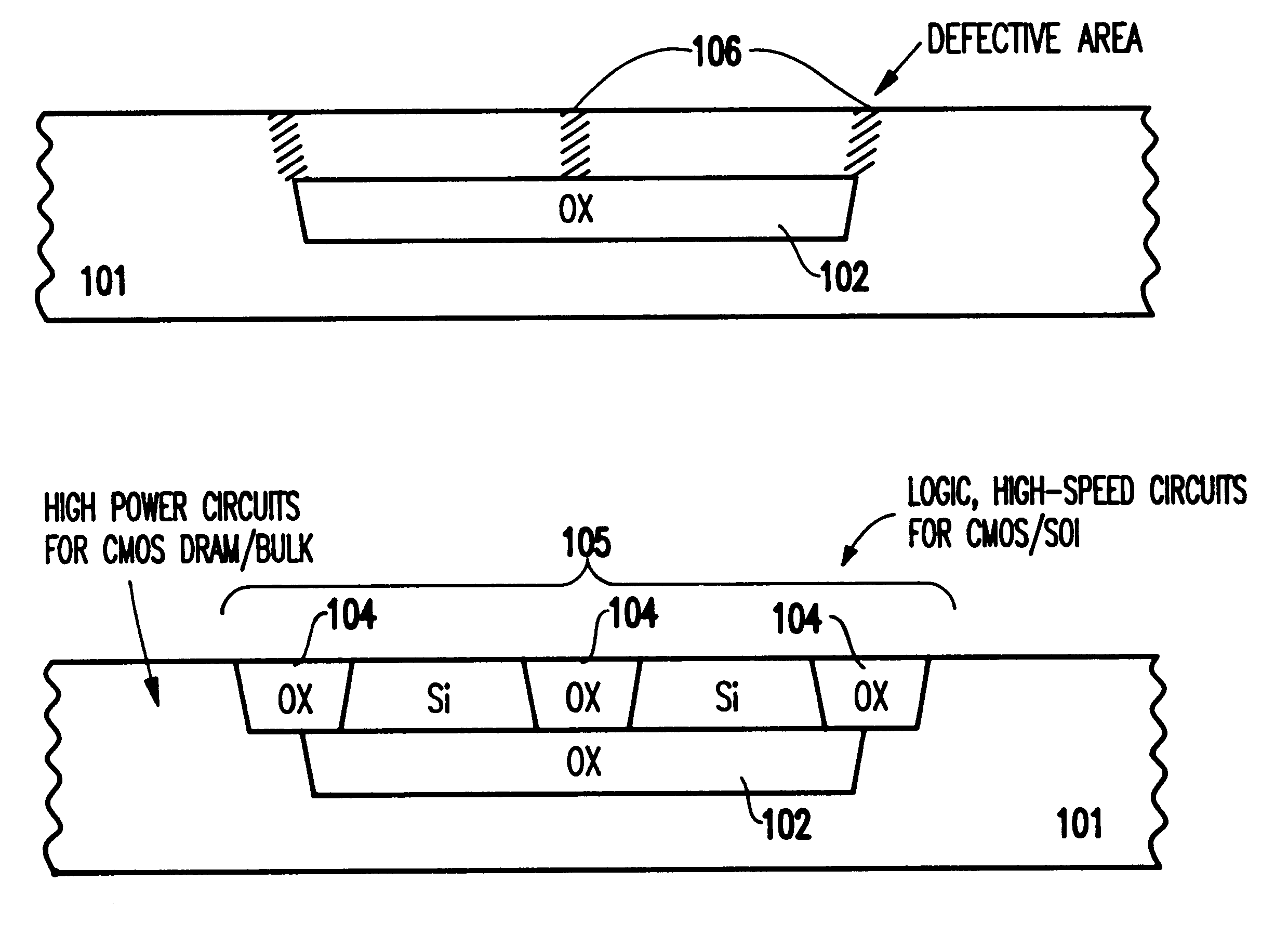
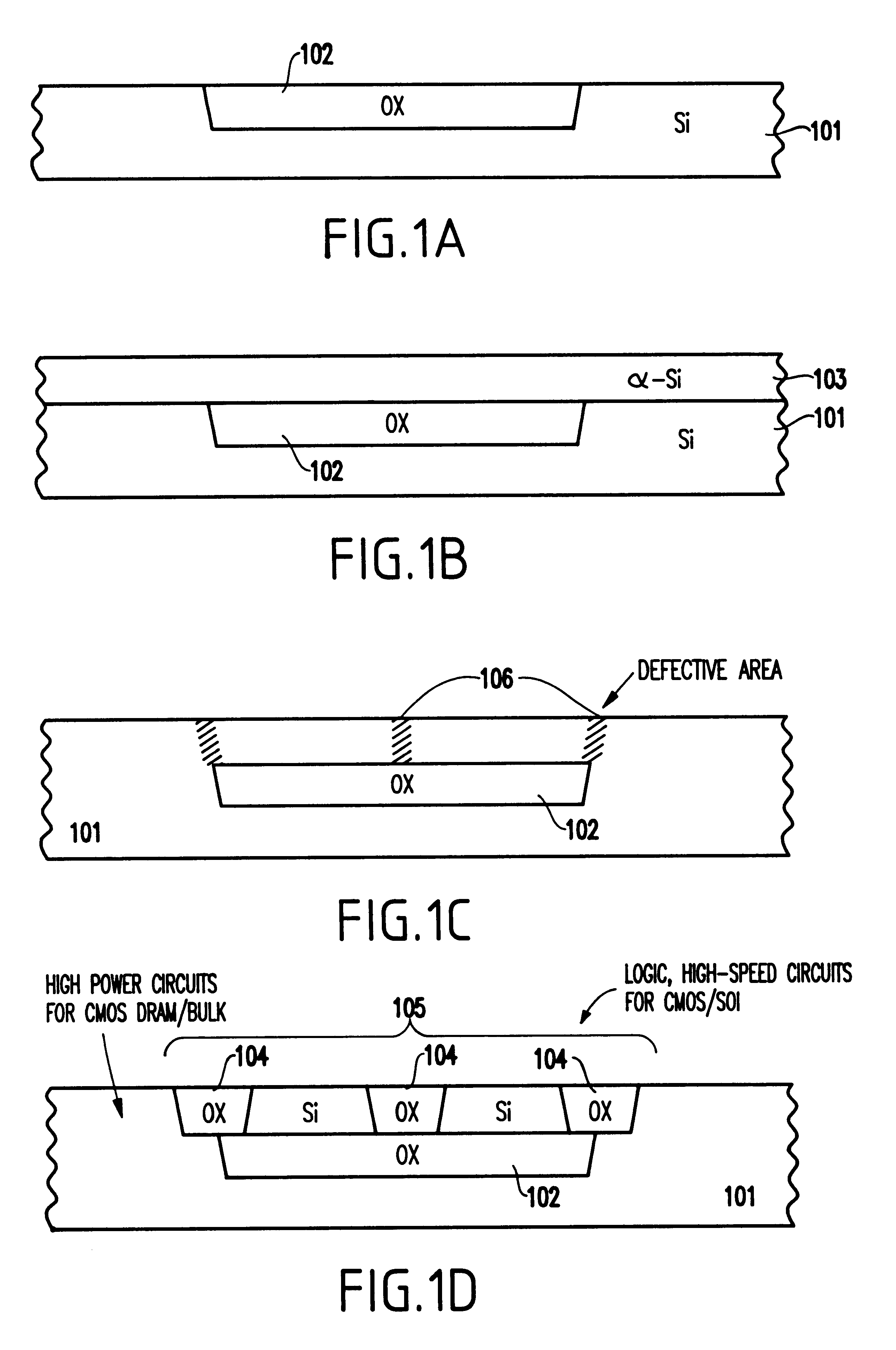
FIGS. 1A-1D illustrate process of forming a substrate for mixed SOI and bulk applications according to a first embodiment of the present invention. Basically, this process shows how to form a local SOI structure in the bulk substrate including isolation and defect removal steps on the SOI silicon layer.

In FIG. 1A, a buried oxide layer 102 is processed (using the method described above) on a single crystal silicon substrate 101. Specifically, a shallow groove is formed in the silicon bulk substrate 101, and is filled with an oxide layer. Preferably, the groove has dimensions of about 2 .mu.m to about 10 .mu.m in width, and 1000 .ANG. to 5000 .ANG. in height / thickness.

Thereafter, as shown in FIG. 1B, an amorphous silicon layer 103 is formed (e.g., deposited) over the oxide 102 and silicon layer 101.

In FIG. 1C, a process is performed to crystalize the amorphous silicon layer using the single silicon crystal substrate as the seeding. Also shown areas in the crystallized layer where defe...

second embodiment

Referring to FIGS. 4A-4D, a method according to a second embodiment of the present invention will be described. A difference between the second embodiment is not planarized as in the first embodiment, and thus is not believed to be as preferred as the first embodiment. However, processing costs are reduced with the second embodiment.

In FIG. 4A, a dielectric (e.g. oxide, nitride) 402 is deposited to a thickness of about 500 .ANG. to about 3000 .ANG., and more preferably to about 1000 .ANG.. Then, the dielectric 402 is patterned through a dry etch or the like. The corner of the patterned dielectric is rounded by dipping in a buffered hydrofluoric (BHF) solution. The rounded corner of the dielectric layer will improve the silicon quality later in the subsequent lateral over-grown epitaxial process.

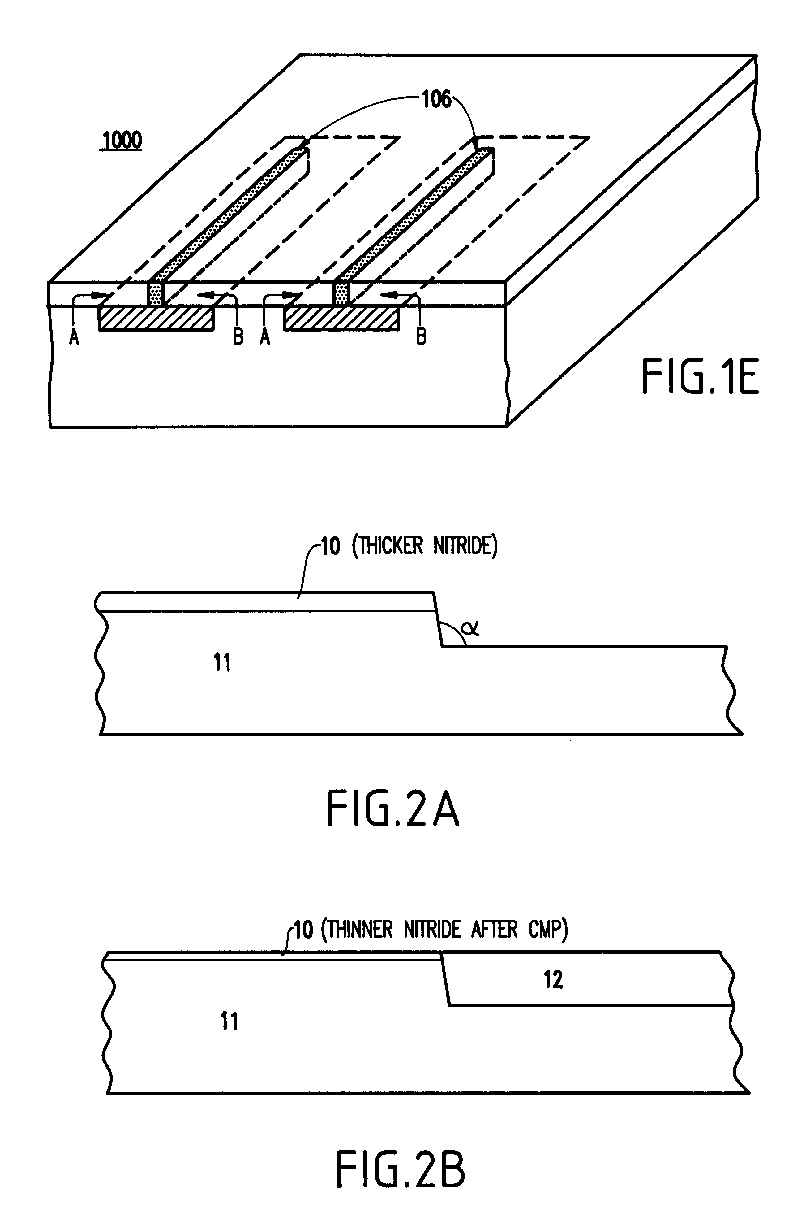
As shown in FIG. 4B, an epitaxial lateral over growth is performed in a manner known in the art. Arrow A shows the vertical growth and arrows B illustrate the horizontal epitaxial growth dire...


PUM


Abstract

A method of forming a semiconductor substrate (and the resulting structure), includes etching a groove into a bulk silicon substrate, forming a dielectric in the groove and planarizing the silicon substrate to form at least one patterned dielectric island in the silicon substrate, forming an amorphous silicon (or SiGe) layer on exposed portions of the silicon substrate and the at least one dielectric island, crystallizing the amorphous silicon (or SiGe) layer using the exposed silicon substrate as a seed, the silicon substrate having direct contact with the formed silicon layer serving as a crystal growth seeding for the crystallization process, and converting the silicon (or SiGe) layer to crystallized silicon, and performing a shallow trench isolation (STI) process, to form oxide isolations between devices.

Description

1. Field of the InventionThe present invention generally relates to a method of forming a semiconductor device, and more particularly to a method of fabricating complementary metal oxide semiconductor (CMOS) devices on a mixed bulk and SOI substrate on the same chip.2. Description of the Related ArtUsing merged dynamic random access memory (DRAM) and logic technology to fabricate a system on a semiconductor chip (e.g., so-called "system-on-chip" (SOC)) has many advantages including reduction of memory latency, larger bandwidth, high-speed processing, and cost reduction.For deep submicron CMOS logic devices, it is advantageous to build the circuits on silicon on insulator (SOI) substrate to improve the performance. However, due to the buried oxide structure and processing techniques used to form an SOI substrate, many devices cannot be built easily on the SOI substrate. For example, a large capacitor on SOI will have a difficult time making contact to the ground node. As another exam...

Claims


Application Information

Patent Timeline
IPC IPC(8): H01L21/70H01L21/762H01L21/84H01L21/02H01L21/20
CPCH01L21/76264H01L21/84H01L21/2022H01L21/76283H01L21/02381H01L21/0243H01L21/02532H01L21/02675H01L21/02689
Inventor CHEN, HOWARD H.HSU, LOUIS L.WANG, LI-KONG
Owner GLOBALFOUNDRIES INC
Learn More