
Method of fabricating a circuit arrangement with thermal vias

a technology of thermal vias and circuits, applied in sustainable manufacturing/processing, laminating printed circuit boards, semiconductor/solid-state device details, etc., can solve the problems of electrical short circuits to the metallic cooling body, damage or completely break through the electrical insulating layer, and negatively affecting the reliability of the thermal closure or sealing

Inactive Publication Date: 2001-02-20
DAIMLER AG
View PDF6 Cites 76 Cited by
  • Summary
  • Abstract
  • Description
  • Claims
  • Application Information

AI Technical Summary

Benefits of technology

When the subsequent soldering process, for example a reflow soldering process, is carried out for mounting the components of the circuit arrangement on the top surface of the substrate, the printed closure or sealing of the via holes prevents the molten solder material from permeating through the via holes from the top surface to the bottom surface of the substrate, and thereby protects the bottom surface of the substrate from soiling or damage that would otherwise be caused by the molten solder. Nonetheless, the heat transport from the top surface to the bottom surface of the substrate through the thermal vias is not significantly diminished by the screen printed material that seals the thermal via holes. This is especially true if the screen printed material is confined to the opening of the via hole and does not overlap onto the rim of the metallization layer around the opening of the hole, or if any such overlap has a limited thickness.
The present invention provides a reliable and simple method for producing circuit arrangements, which can completely prevent the flow or penetration of solder material through the thermal vias provided in the substrate. The present method can be carried out with a low cost and completely independently of the particular embodiment of the thermal vias, for example independently of the type and configuration of the through-contacts provided in the thermal vias. The present method can be successfully and reliably carried out without diminishing the thermal transfer through the thermal vias even for relatively large diameters of the thermal vias, for example for via diameters in a range from 0.4 mm to 1 mm.

Problems solved by technology

Once the molten metal material reaches the bottom surface of the supporting substrate, it damages or completely breaks through the electrical insulating layer such as an insulating film applied on the bottom surface of the supporting substrate.
This results in electrical short circuits to the metallic cooling body or to a metal housing or the like that supports or encloses the substrate as well as the circuit arrangement.
Otherwise, such bubbles or cracks would negatively influence the reliability of the closure or seal of the thermal via holes provided by the screen printed material.

Method used


Image

  • Method of fabricating a circuit arrangement with thermal vias
  • Method of fabricating a circuit arrangement with thermal vias

Examples


Embodiment Construction

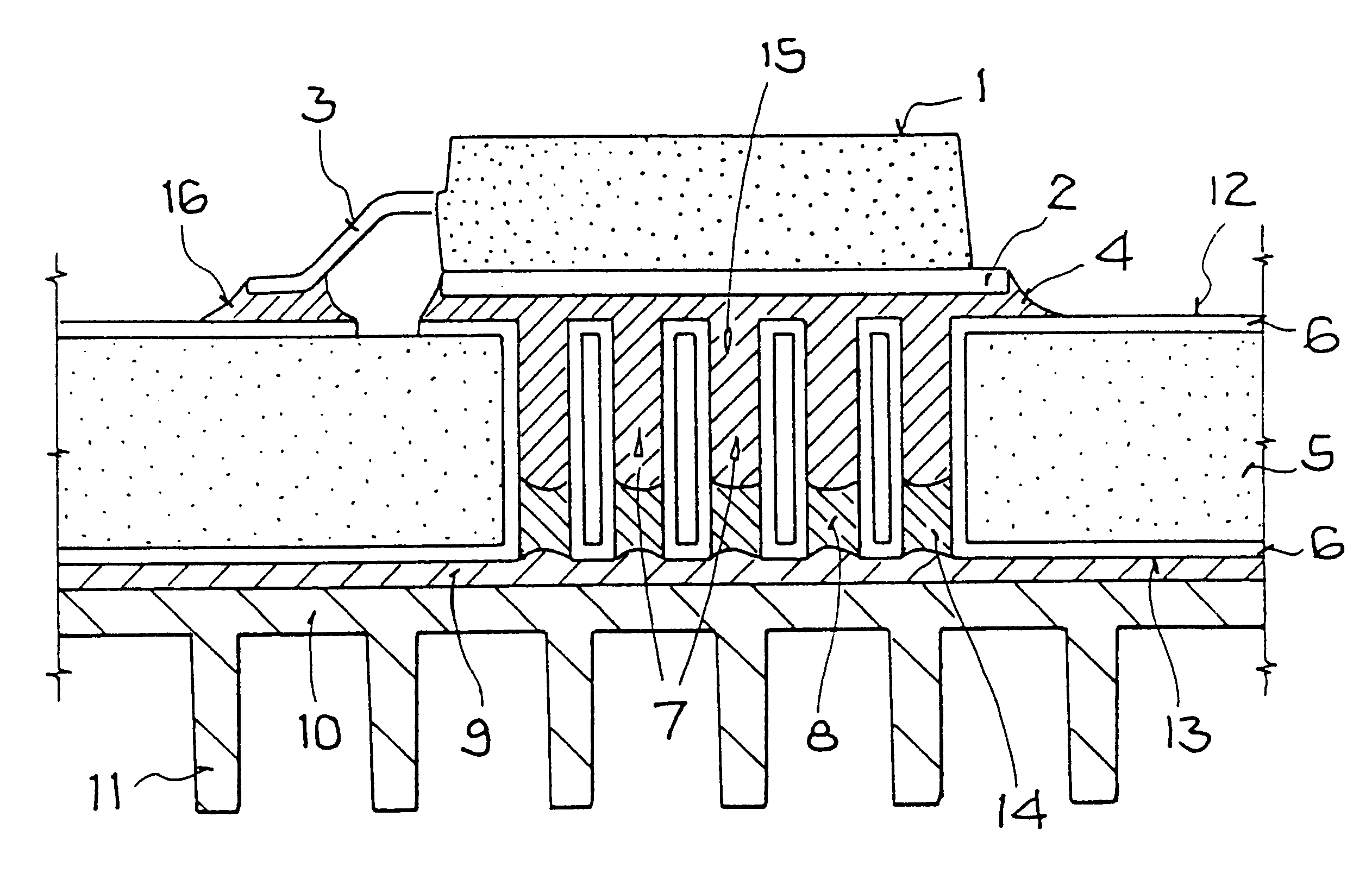
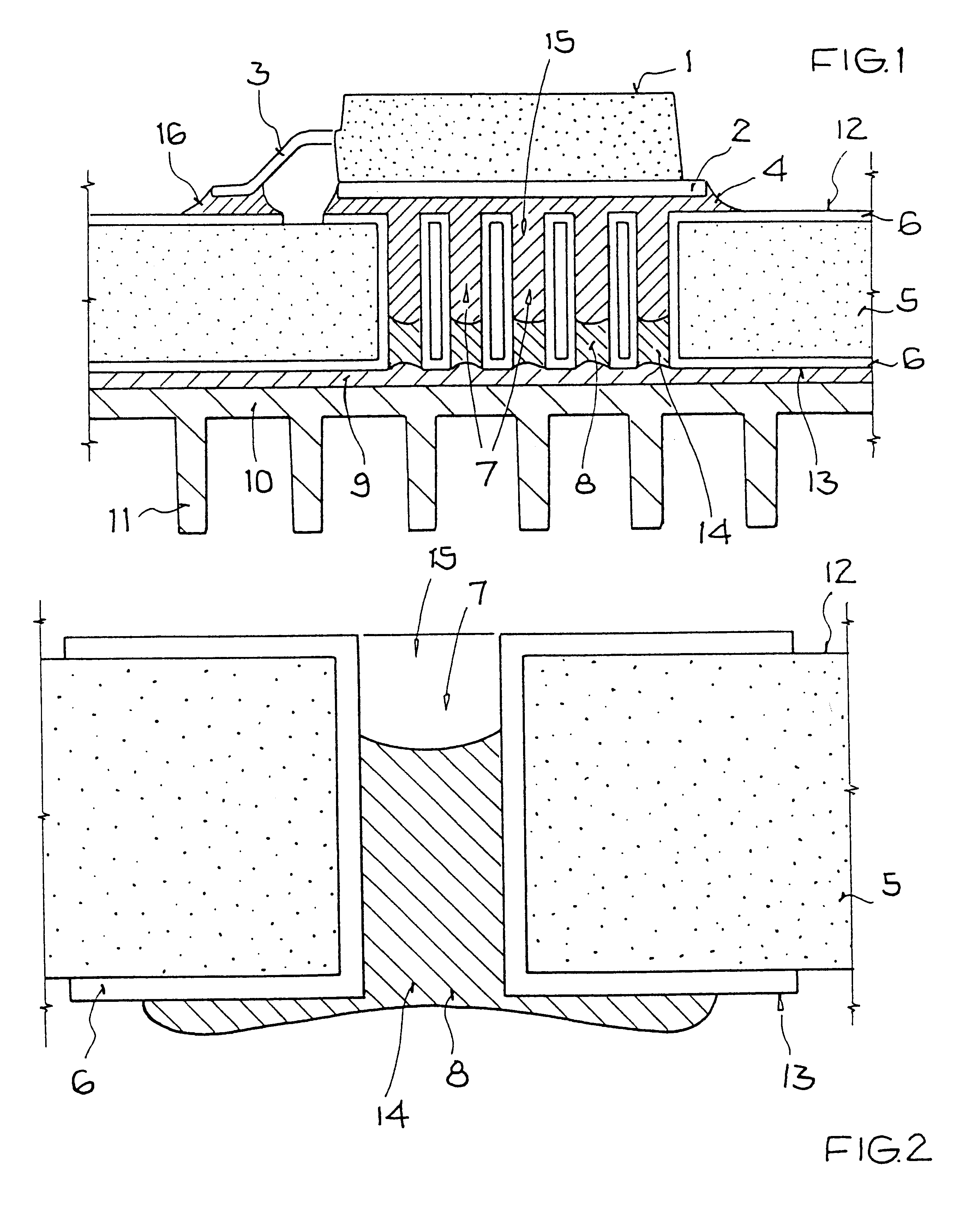
FIG. 1 shows a circuit arrangement including at least one power electronics component 1 in addition to further active and passive components arranged on the top surface 12 of a supporting substrate particularly embodied as a circuit board such as a printed circuit board. The power component 1 has electrical contacts 3 that are to be contacted or electrically connected by means of contact pads 16 to the conductor path arrangement that has been provided on the top surface 12 of the circuit board 5 and that consists of copper coated with a gold-nickel (AuNi) alloy, for example.

During operation of the circuit arrangement, the several components thereof and particularly the power component 1 dissipates power in the form of heat which must be removed from the circuit arrangement to prevent damage and / or improper operation thereof. In order to remove the dissipated heat in a vertical direction, plural through-holes are bored through the circuit board 5 in the areas respectively below the p...


PUM


Abstract

An electronic component is mounted on a substrate such as a circuit board by means of a soldering process such as reflow soldering. The circuit board has a thermal via hole therethrough to provide a heat dissipation path from the top surface to the bottom surface of the circuit board, for dissipating heat from the electronic component. To prevent molten solder from penetrating through the via hole during the soldering process, the via hole is sealed prior to the soldering process. The via hole is sealed from the bottom surface of the substrate by carrying out a screen printing process including at least two printing passes to print a sealing material into the open hole of the thermal via.

Description

PRIORITY CLAIMThis application is based on and claims the priority under 35 U.S.C. .sctn.119 of German Patent Application 198 42 590.2, filed on Sep. 17, 1998, the entire disclosure of which is incorporated herein by reference.1. Field of the InventionThe invention relates to a method of fabricating a circuit arrangement, for example including a surface mount device mounted on a printed circuit board, having thermal through-hole contacts or vias provided through the circuit board.2. Background InformationMany electronics applications utilize electronic circuit arrangements including electronic components that generate a rather high power dissipation and therefore heat dissipation during operation. This is especially true in circuit arrangements including power components such as power modules for controlling and driving other assemblies or the like. The various components of the circuit arrangement are typically mounted on a suitable support body or substrate. For example, in the fi...

Claims


Application Information

Patent Timeline
Patent Type & Authority Patents(United States)
IPC IPC(8): H05K3/34H05K3/00H05K1/02H05K7/20H05K3/12H05K1/11
CPCH01L23/3677H05K1/0206H05K3/0094H05K3/341H05K7/205H05K7/20854H05K1/113H05K3/0058H05K3/1216H05K3/3452H05K2201/066H05K2201/09572H05K2201/0959H05K2201/10166H05K2201/10969H05K2203/1476H01L2924/0002H01L2924/00Y02P70/50
Inventor HEINZ, HELMUTSCHUCH, BERNHARD
Owner DAIMLER AG
Learn More