
Controlled pore ceramics chips for high throughput solid state oligonucleotide synthesis

Pending Publication Date: 2022-11-10
NANOPEC INC
View PDF0 Cites 0 Cited by
  • Summary
  • Abstract
  • Description
  • Claims
  • Application Information

AI Technical Summary

Benefits of technology

This patent describes a new type of ceramic film that can be used to make oligonucleotides (DNA and RNA). These films are made without using heavy metals and are stable under the conditions used in DNA synthesis. They are also much smaller than commonly used silicon chips, which means they can handle larger amounts of oligonucleotides. This makes them a potential cost-effective replacement for current materials. Additionally, they can be easily activated and have uniform surfaces for chemical printing. These ceramic films have shown promising results in chemical testing and are expected to be better than silicon chips for making oligonucleotides.

Problems solved by technology

Extracellular (in vitro) DNA amplification or gene synthesis—physically creating artificial gene sequences using the polymerase chain reaction and other enzymes in solution, is slow and prone to errors.
Controlled pore glass (CPG) columns lacks the quality necessary to create long sequences.
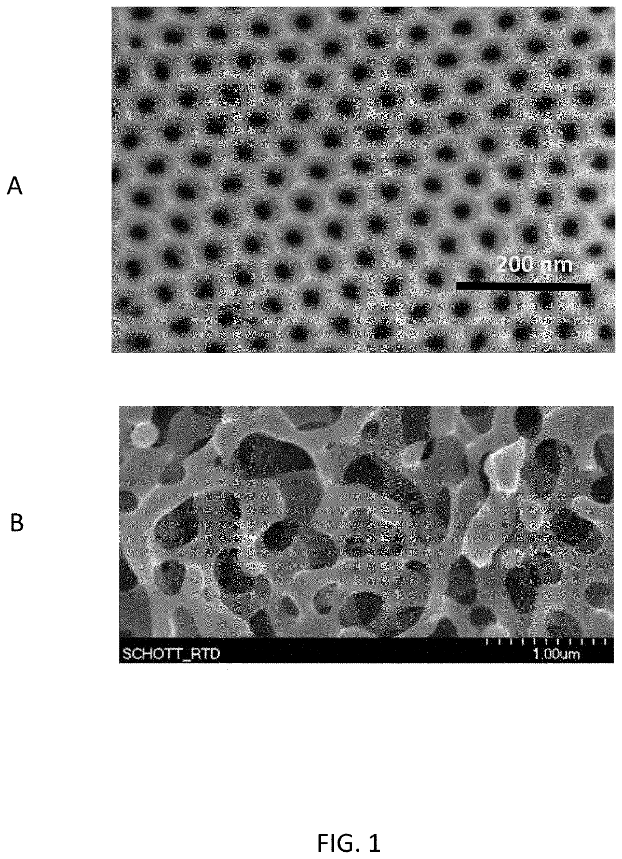
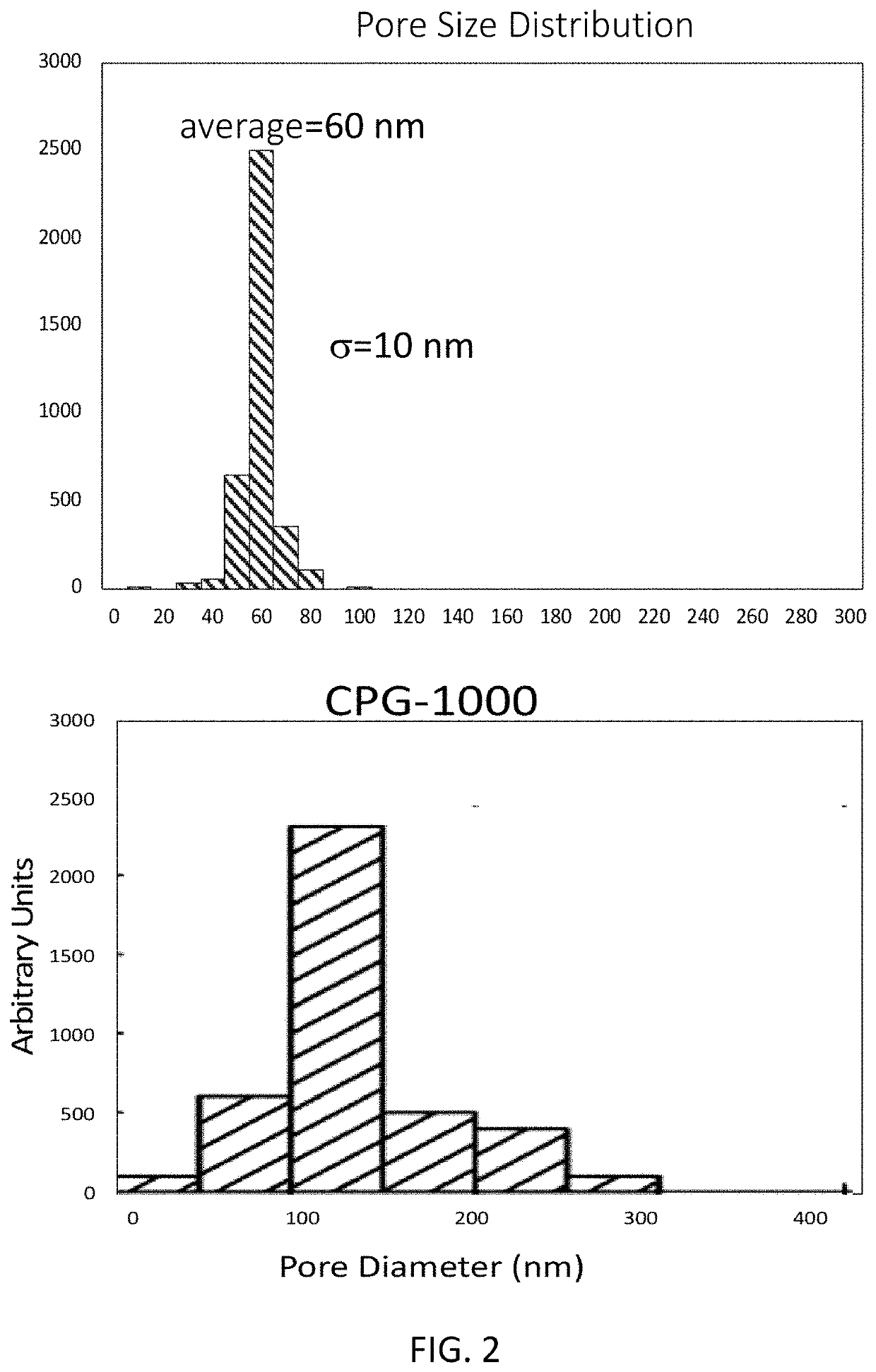
This is due in great part to the broad particle size distribution which leads to incomplete synthesis of oligonucleotides trapped in small spaces (“shortmers”).
In addition, CPG columns are too large and difficult to scale for the hundreds if not thousands of sequences needed to generate a full gene.
Because the amount of surface area for reactions on silicon chips have physical limitations yield of these chips is very low.
Increasing the surface area with nano-lithography is possible but extremely expensive.
This is a key bottleneck for high-throughput and inexpensive synthetic gene and genome construction.
Materials with these qualities cannot be made with inexpensive polymers which tend to swell in the presence of solvents.
Most semiconductor materials require expensive nano-lithography to add sufficient surface area for high loading.

Method used


Image

  • Controlled pore ceramics chips for high throughput solid state oligonucleotide synthesis
  • Controlled pore ceramics chips for high throughput solid state oligonucleotide synthesis
  • Controlled pore ceramics chips for high throughput solid state oligonucleotide synthesis

Examples


example 1

[0079]A major oligonucleotide independent laboratory provided loadings on DNAReax and compared them to CPG. Loadings of 200 nanomoles where achieved on a circular ceramic chip 20 mm in diameter. On a volume basis this is comparable to CPG but on a weight basis (DNAReax is 1.89 g / cc compared with CPG 0.4 g / cc) this is around 20% loading by weight.

example 2

[0080]A DNA synthesis laboratory conducted tests on columns packed with DNA chips. Two batches having two columns each were tested. The loads varied between 15.8 to 21.9 nanomoles / cm2 of DNAReax chip surface. On a weight basis this represents around 15% of the expected loads for their internal CPG column standards on a weight basis. Compared with state-of-the-art chip yields however this represent between 300% to 400% higher yields.

example 3

[0081]A different independent laboratory was asked to compare oligonucleotide loads on DNAReax with silicon chips used by the industry. An oligonucleotide with 30 bases was synthesized on DNAReax chips. Two separate batches of three chips each were tested. On average these batches gave yields between 4.9 and 8.3 nanomoles / cm2. These loads are 70 times higher than on silicon chips.


PUM


Abstract

A nano-structured ceramic film with controlled pore size for the high throughput synthesis of oligonucleotides (DNA and RNA). The film can be cut into chips of predetermined size, and code printed for optical recognition in automated DNA synthesizers. The chips are easily activated under very mild conditions and silanization proceeds uniformly to allow reagents to flow unhindered through its open pores. Mono layer modifications, such as covalently bound silane coupling agents, allows for the addition of universal linkers and improved yields compared to conventional approaches.

Description

CROSS-REFERENCE TO RELATED APPLICATIONS[0001]The present application claims priority to U.S. Provisional Application No. 63 / 183,723 filed on May 4, 2021.BACKGROUND OF THE INVENTION1. Field of the Invention[0002]The present invention relates to nanostructured ceramic films and, more specifically, to a nano-structured ceramic film with controlled pore size providing a chemically, optically and mechanically robust substrate for high-throughput solid state manufacturing of synthetic oligonucleotides.2. Description of the Related Art[0003]DNA synthesis occurs in all eukaryotes and prokaryotes. The molecular in vivo machinery involved in DNA synthesis has been studied extensively since the 1950's. The accurate synthesis of DNA is important in order to avoid mutations to DNA which could lead to diseases such as cancer. DNA biosynthesis in nature occurs via the polymerase chain reaction. In vivo DNA polymerases are highly accurate, with an intrinsic error rate of less than one mistake for e...

Claims


Application Information

Patent Timeline
IPC IPC(8): B01J19/00C07H21/00C40B40/06B82Y30/00
CPCB01J19/0046C07H21/00C40B40/06B82Y30/00B01J2219/00722B01J2219/00596B01J2219/00585B01J2219/00659B01J2219/00725B01J2219/00587B01J2219/00608B01J2219/00612B01J2219/00619B01J2219/00621B01J2219/00632B01J2219/00641
Inventor BLANCO, MARIO
Owner NANOPEC INC
Learn More