Trench field effect transistor structure and manufacturing method thereof

Pending Publication Date: 2022-10-13
CHINA RESOURCES MICROELECTRONICS (CHONGQING) CO LTD
View PDF0 Cites 1 Cited by
  • Summary
  • Abstract
  • Description
  • Claims
  • Application Information

AI Technical Summary

Benefits of technology

This patent describes a method of manufacturing a trench field effect transistor (TET) that has a smaller cell unit pitch, higher cell density, and lower device channel resistance compared to existing methods. The method uses a self-alignment process, which allows for easier placement of the source and drain electrodes. Additionally, a "T"-shaped structure is used for the source electrode, which increases the contact area with the source and body region, reducing the source contact resistance and improving the device's avalanche tolerance. Overall, this method provides a stable electrical parameter and low specific on-resistance for the resulting device structure.

Problems solved by technology

Limitation of the traditional process makes it difficult to effectively reduce the device cell pitch continuously.
In addition, to maintain a safe process production window, it is required to maintain a certain safety distance between the bottom of a source contact hole and a device channel, and if the alignment accuracy of the lithography machine cannot ensure that a distance between the bottom of the source contact hole and the device trench is beyond the safety distance, an effective concentration of a surface of the device channel would increase, resulting in increasing of a device on voltage and increasing of a device channel resistance.
As a result, the specific on-resistance of the device increases, and an electrical parameter of the device would be unstable.
Moreover, due to that the shielding gate trench MOSFET structure requires a shielding gate oxide layer with a particular thickness and a shielding gate polycrystalline silicon, and due to the process capability limitation and the device structure requirement, it is difficult for a conventional shielding gate trench MOSFET structure to implement a product with a stable electrical parameter and a relatively small cell unit pitch that can meet the performance of the device.

Method used


Image

  • Trench field effect transistor structure and manufacturing method thereof
  • Trench field effect transistor structure and manufacturing method thereof
  • Trench field effect transistor structure and manufacturing method thereof

Examples


Embodiment Construction

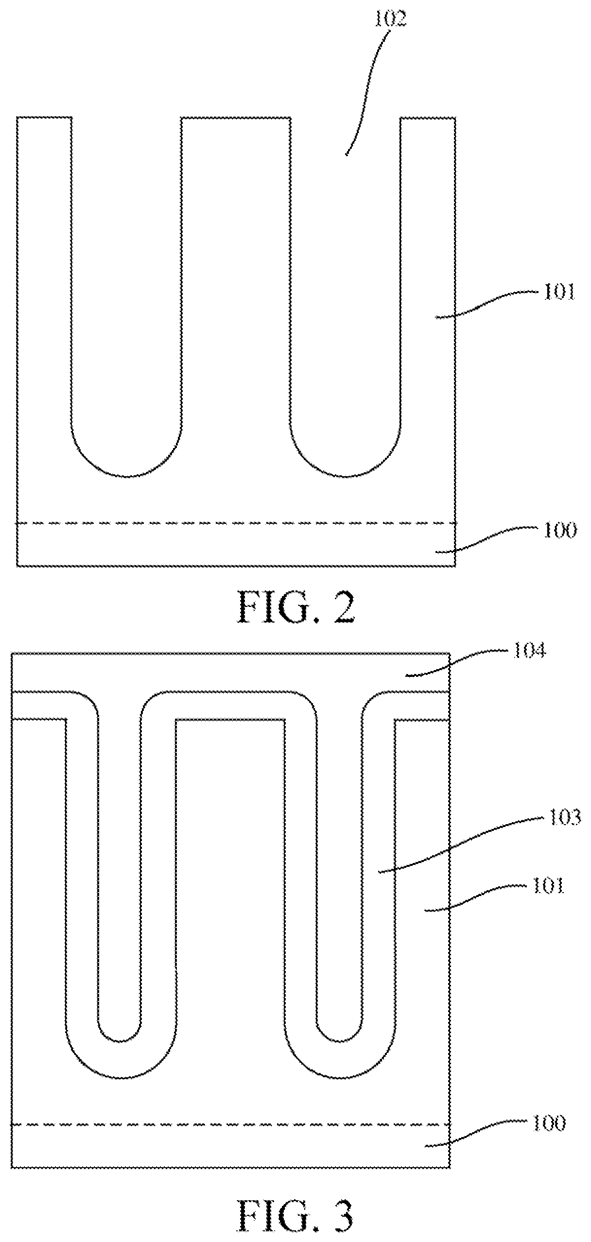
[0044]As shown in FIG. 1, the present disclosure provides a manufacturing method for a trench field effect transistor structure, including the following steps:

[0045]providing a substrate of a first doping type, forming an epitaxial layer of the first doping type on the substrate, and forming a plurality of device trenches in the epitaxial layer;

[0046]forming a shielding dielectric layer on an inner wall of the device trench, forming a shielding gate layer on a surface of the shielding dielectric layer, filling at least the bottom of the device trench with the shielding gate layer, and forming a first isolation dielectric layer on the shielding gate layer, where the first isolation dielectric layer and the shielding dielectric layer surround the shielding gate layer;

[0047]forming a gate dielectric layer on at least side walls of the device trench and the first isolation dielectric layer, so that a gate trench is defined by a surface of the gate dielectric layer, and filling the gate ...


PUM


Abstract

The present disclosure provides a trench field effect transistor structure and a manufacturing method thereof. The manufacturing method includes: providing a substrate (100), forming an epitaxial layer (101), forming a device trench (102) in the epitaxial layer, and forming a shielding dielectric layer (107), a shielding gate layer (105), a first isolation dielectric layer (108), a gate dielectric layer (109), a gate layer (110), a second isolation dielectric layer (112), a body region (114), a source (115), a source contact hole (118), a source electrode structure (122), and a drain electrode structure (123). During manufacturing of a trench field effect transistor structure, a self-alignment process is adopted in a manufacturing process, so that a cell pitch is not limited by an exposure capability and alignment accuracy of a lithography machine, to further reduce the cell pitch of the device, improve a cell density, and reduce a device channel resistance.

Description

TECHNICAL FIELD[0001]The present disclosure relates to a power semiconductor technology, and in particular, to a trench field effect transistor structure and a manufacturing method thereof.BACKGROUND[0002]A shielding gate trench metal-oxide-semiconductor field-effect transistor (MOSFET) device has the advantages of a lower on resistance, a faster switching speed, and the like than a conventional trench MOSFET, and is widely used in the fields such as switching power supply, AC-AC conversion, motor control, radio frequency communication, uninterruptible power supply, and frequency converter. To obtain a high conversion efficiency application system, it is necessary to continuously reduce a switching loss and a conduction loss of the shielding gate trench MOSFET. Reducing the conduction loss means to reduce a specific on-resistance of the shielding gate trench MOSFET.[0003]The most effective method for reducing the specific on-resistance of the shielding gate trench MOSFET is to reduc...

Claims


Application Information

Patent Timeline
IPC IPC(8): H01L29/66H01L29/10H01L29/40H01L29/417H01L29/78H01L21/265
CPCH01L29/66727H01L29/1095H01L29/407H01L29/41741H01L29/7813H01L21/26513H01L29/66734H01L29/66666H01L29/7827H01L29/401H01L29/4236H01L29/41766H01L29/66719H01L29/66712H01L29/7802H01L29/41725H01L29/66621H01L29/0696
Inventor YAO, XINJIAO, WEILIU, HUARUILV, PING
Owner CHINA RESOURCES MICROELECTRONICS (CHONGQING) CO LTD
Why Eureka
Try Eureka