Schottky diode and preparation method thereof

A technology of Schottky diodes and doped layers, applied in semiconductor/solid-state device manufacturing, semiconductor devices, electrical components, etc., can solve problems such as low on-resistance of on-channel channels

Pending Publication Date: 2021-06-04
GUANGHUA LINGANG ENG APPL & TECH R&D (SHANGHAI) CO LTD
View PDF0 Cites 1 Cited by
  • Summary
  • Abstract
  • Description
  • Claims
  • Application Information

AI Technical Summary

Problems solved by technology

[0004] The technical problem to be solved by the present invention is to overcome the problem in the prior art that it is impossible to ensure that the conduction channel is completely pinched off at a small reverse bias voltage and has a low on-resistance during forward conduction.

Method used


Image

  • Schottky diode and preparation method thereof
  • Schottky diode and preparation method thereof
  • Schottky diode and preparation method thereof

Examples


preparation example Construction

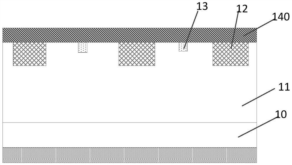
[0074] Correspondingly, another embodiment of the present invention also provides a method for preparing a Schottky diode, referring to Figure 6 , including the following steps:

[0075] S01: providing a semiconductor substrate layer;

[0076] S02: forming a drift layer on the semiconductor substrate layer, the drift layer includes a first drift region and a second drift region located on the side of the first drift region facing away from the semiconductor substrate layer, the second drift region a doping concentration greater than that of the first drift region;

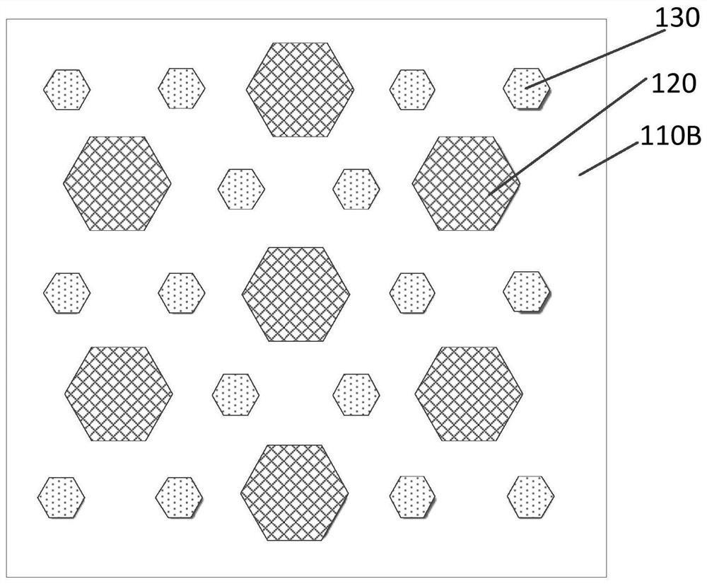
[0077] S03: forming a sub-doped layer in part of the second drift region, the conductivity type of the sub-doped layer is opposite to the conductivity type of the drift layer;

[0078] S04: Form several main doped layers in the drift layer, several main doped layers are spaced around the sub-doped layer, the conductivity type of the main doped layer is the same as the conductivity type of the sub-doped layer . ...


PUM

PropertyMeasurementUnit
areaaaaaaaaaaa

Abstract

The invention discloses a Schottky diode and a preparation method thereof. The Schottky diode comprises a semiconductor substrate layer; a drift layer is located on the semiconductor substrate layer and comprises a first drift region and a second drift region, the second drift region is located on the side, opposite to the semiconductor substrate layer, of the first drift region, and the doping concentration of the second drift region is larger than that of the first drift region; an auxiliary doping layer is located in a part of the second drift region, and the conduction type of the auxiliary doping layer is opposite to that of the drift layer; a number of main doping layers are located in the drift layer and distributed around the auxiliary doping layer at intervals, and the conduction type of the main doping layers is the same as that of the auxiliary doping layer. The Schottky diode ensures that a conducting channel is completely pinched off when the reverse bias voltage is relatively small, and meanwhile, the Schottky diode can ensure that the Schottky diode has low on-resistance when the Schottky diode is in forward conduction.

Description

technical field [0001] The invention relates to the field of semiconductors, in particular to a Schottky diode and a preparation method thereof. Background technique [0002] Power diode is one of the most commonly used electronic components and the most basic unit of power electronic circuits. Its unidirectional conductivity can be used for rectification, clamping and freewheeling of circuits. The diode in the peripheral circuit mainly plays an anti-reverse function to prevent device damage caused by current reverse injection. Traditional power diodes mainly include Schottky power diodes and PN junction power diodes. Compared with PN junction power diodes, Schottky power diodes use metal-semiconductor contacts (gold half-contacts) to form metal-semiconductor junctions, making their forward turn-on voltage smaller. Moreover, the Schottky power diode is a unipolar majority carrier conduction mechanism, its reverse recovery time is ideally zero, and there is no accumulation ...

Claims


Application Information

Patent Timeline
Patent Type & Authority Applications(China)
IPC IPC(8): H01L29/872H01L29/06H01L29/36H01L21/329
CPCH01L29/872H01L29/0607H01L29/0684H01L29/36H01L29/6606
Inventor 张园览张清纯
Owner GUANGHUA LINGANG ENG APPL & TECH R&D (SHANGHAI) CO LTD
Why Eureka
Try Eureka