Semiconductor light emitting device

Pending Publication Date: 2021-10-21
SONY SEMICON SOLUTIONS CORP
View PDF0 Cites 0 Cited by
  • Summary
  • Abstract
  • Description
  • Claims
  • Application Information

AI Technical Summary

Benefits of technology

The present disclosure relates to a semiconductor light emitting device that improves light emission characteristics. The device includes a nitride semiconductor substrate with two layers of different dislocation direction, which serve as an underlayer and are arranged on the substrate with the principal plane inclined from the c-plane in the m-axis direction. This results in a more lattice-relaxed underlayer and improved crystal quality of the active layer, which in turn provides better light emission characteristics.

Problems solved by technology

This leads to a higher lattice mismatch degree, causing a crystal defect or dislocation to be introduced to thereby degrade the crystallinity.

Method used


Image

  • Semiconductor light emitting device
  • Semiconductor light emitting device
  • Semiconductor light emitting device

Examples


embodiment

1. Embodiment

[0023](An example in which two layers that are different from each other in dislocation direction in the layer are provided as underlayers on a substrate)

[0024]1-1. Configuration of Semiconductor Laser

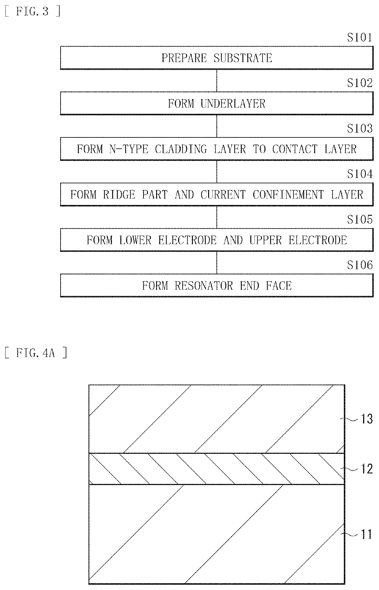
[0025]1-2. Manufacturing Method of Semiconductor Laser

[0026]1-3. Workings and Effects

2. Modification Example

[0027](An example in which respective intermediate layers are provided between the substrate and a first underlayer, between the first underlayer and a second underlayer, and between the second underlayer and a device layer)

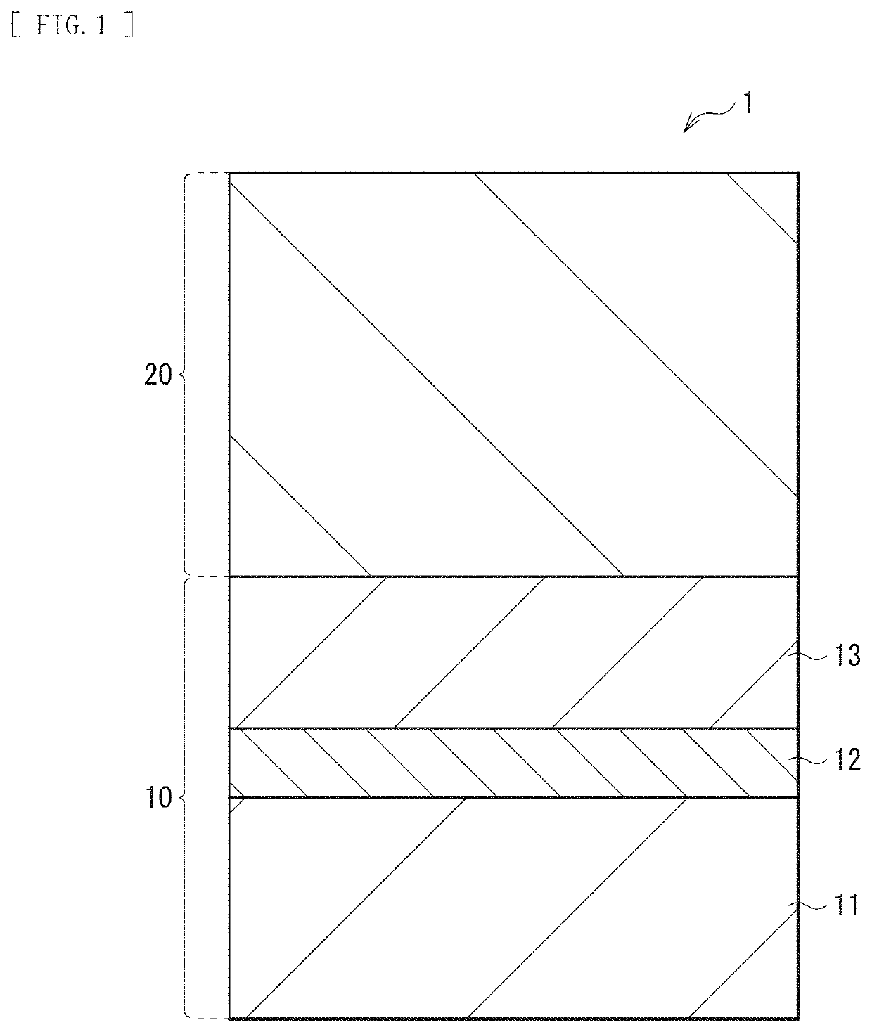
[0028]FIG. 1 schematically illustrates a cross-sectional configuration of a semiconductor light emitting device (a semiconductor light emitting device 1) according to an embodiment of the present disclosure. The semiconductor light emitting device 1 is, for example, a semiconductor laser (LD), a light emitting diode (LED), or the like that emits light in a visible region, particularly, with a wavelength of 480 nm or more. The semiconductor light e...

modification example

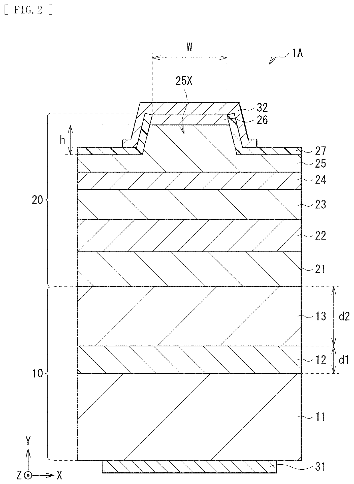
[0058]FIG. 7 schematically illustrates a cross-sectional configuration of a semiconductor light emitting device (a semiconductor light emitting device 2) according to an embodiment of the disclosure. The semiconductor light emitting device 2 is, as in the foregoing embodiment, a semiconductor laser (LD), a light emitting diode (LED), or the like that emits light in a visible region, particularly, with a wavelength of 480 nm or more, for example. Like the semiconductor light emitting device 1, the semiconductor light emitting device 2 of the present modification example has a configuration in which the device layer 20 (a device) including an active layer (for example, the active layer 23) is provided on a template substrate 40 in which the first underlayer 12 and the second underlayer 13 are stacked in this order on the substrate 11 having, as the principal plane, a plane inclined from the c-plane in the m-axis direction in the range from 60° to 90° both inclusive. The present modifi...


PUM


Abstract

A semiconductor light emitting device of an embodiment of the present disclosure includes: a nitride semiconductor substrate having, as a principal plane, a plane inclined from a c-plane in an m-axis direction in a range from 60° to 90° both inclusive; an underlayer provided on the nitride semiconductor substrate and including a first layer and a second layer that are stacked on each other, the first layer including Alx2Inx1Ga(1-x1-x2)N (0<x1<1, 0≤x2<1) and having a dislocation along an intersection line of the principal plane of the nitride semiconductor substrate and a (1-100) plane, the second layer including Aly2Iny1Ga(1-y1-y2)N (0<y1<1, 0≤y2<1) and having a dislocation along an intersection line of the principal plane of the nitride semiconductor substrate and a (0001) plane; and a device layer including an active layer provided on the underlayer.

Description

TECHNICAL FIELD[0001]The present disclosure relates to a semiconductor light emitting device using, for example, a nitride semiconductor material.BACKGROUND ART[0002]Recently, semiconductor lasers (LDs: Laser Diodes) and light emitting diodes (LEDs: Light Emitting Diodes) that use a nitride semiconductor and emit light in a range from a blue band to a green band have been developed actively for use as a light source. Among the above, a semipolar or non-polar nitride semiconductor, which is able to reduce an influence of a piezoelectric field, is effective in configuring a semiconductor light emitting device that emits light in a long wavelength band.[0003]In order to achieve a longer emission wavelength of a semiconductor light emitting device with an active layer including GaInN, it is necessary to increase a content of indium (In). In a case where an active layer having a high In content is crystal-grown on a GaN substrate using a typical method, the active layer having the high I...

Claims


Application Information

Patent Timeline
IPC IPC(8): H01S5/343
CPCH01S5/34333H01S5/22H01L33/32H01L33/16H01S5/0202H01S5/0287H01S5/320275
Inventor NAKAYAMA, YUUSUKE
Owner SONY SEMICON SOLUTIONS CORP
Why Eureka
Try Eureka