Widely tunable, single mode emission semiconductor laser

Pending Publication Date: 2021-10-07
AUTOMOTIVE COALITION FOR TRAFFIC SAFETY
View PDF4 Cites 0 Cited by
  • Summary
  • Abstract
  • Description
  • Claims
  • Application Information

AI Technical Summary

Benefits of technology

The present invention is a widely tunable semiconductor laser that allows for a compact characterization process based on the measurement of only five tuning parameters and a few base wavelengths. The laser can be easily integrated in a photonic integrated circuit and allows for an online calibration mode. The invention has a simple structure and is highly efficient in terms of its tuning range and power consumption. The technical effects of the present invention are that it allows for easier and more accurate laser calibration, and it can be easily integrated into photonic integrated circuits.

Problems solved by technology

There exists a wide range of wavelength selection mechanisms, but fully electronic wavelength selection mechanisms are typically limited to a tuning ratio of r≈0.01 or less.
Wavelength selection mechanisms that support a wider range of wavelengths typically possess a very large parameter space (i.e., they have a large number of tuning parameters), which complicates the characterization process and the controlled operation of these wavelength selection mechanisms, and thus renders these approaches unfeasible for mass production.
The combination of these two effects (continuous tuning and relative tuning) achieve, in principle, much higher tuning ranges but, in practice, fabrication and characterization complexities increase significantly as the tuning range increases.
Those lasers that possess DFB gratings or DBRs and which are able to select more than one wavelength are usually very complex in their operation.
This makes the operating characteristics of the laser very susceptible to variations in the fabrication process.
Finding the desired protocol of operating parameters leads to a very complex characterization process in a high-dimensional parameter space (i.e., it is a highly complex procedure to characterize the particular waveguide material temperature and the particular injected current density for each segment of the laser).
The number of elements of this grid increases exponentially with the number of independent parameters, which makes it unfeasible to fabricate and control DFB or DBR lasers with the number of segments that is necessary to stably select many wavelengths.
Furthermore, known mechanisms that implement wavelength selection through the Vernier tuning principle suffer from a similar problem: since one wants to simultaneously control the output wavelength, output intensity and side mode suppression ratio, one needs many control parameters (in particular, waveguide material temperature and injection current densities).
This again leads to a very complex characterization process in a very high dimensional parameter space, which makes mass production of devices with full simultaneous control of output wavelength, output intensity and side mode suppression ratio unfeasible.

Method used


Image

  • Widely tunable, single mode emission semiconductor laser
  • Widely tunable, single mode emission semiconductor laser
  • Widely tunable, single mode emission semiconductor laser

Examples


Embodiment Construction

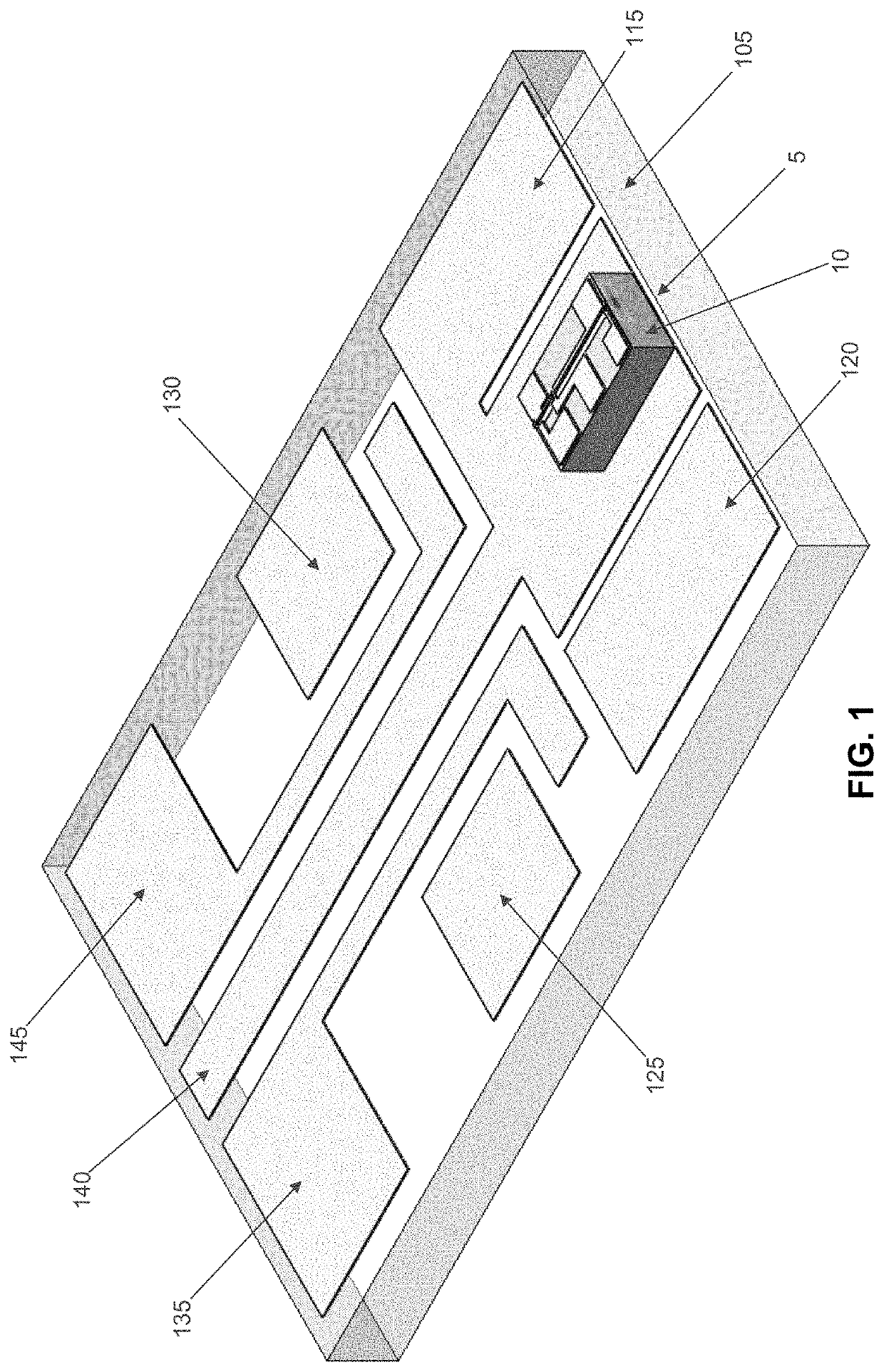
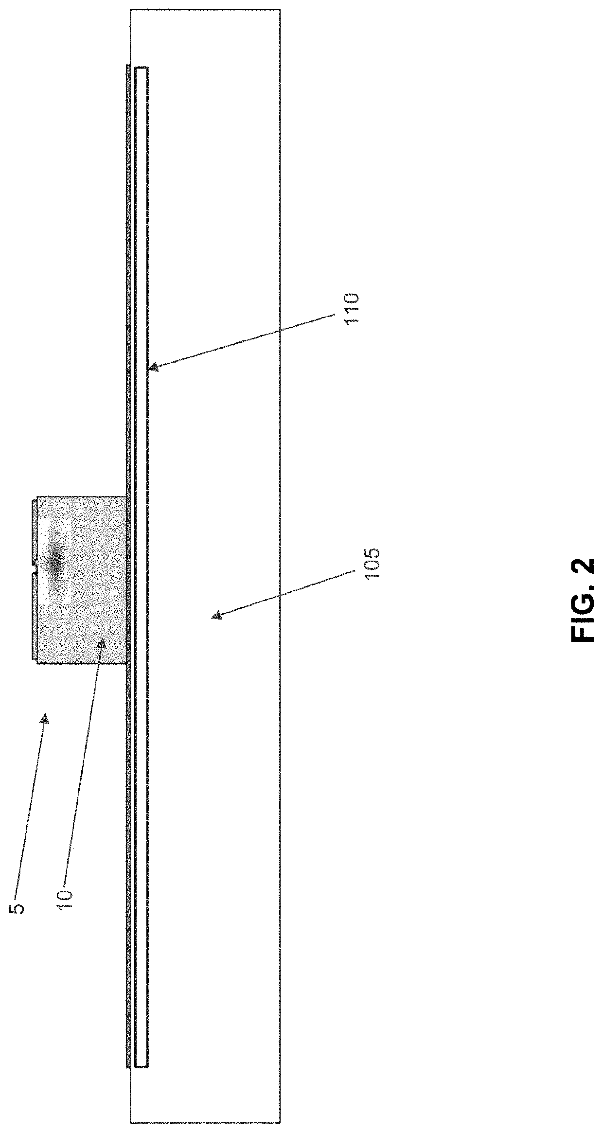
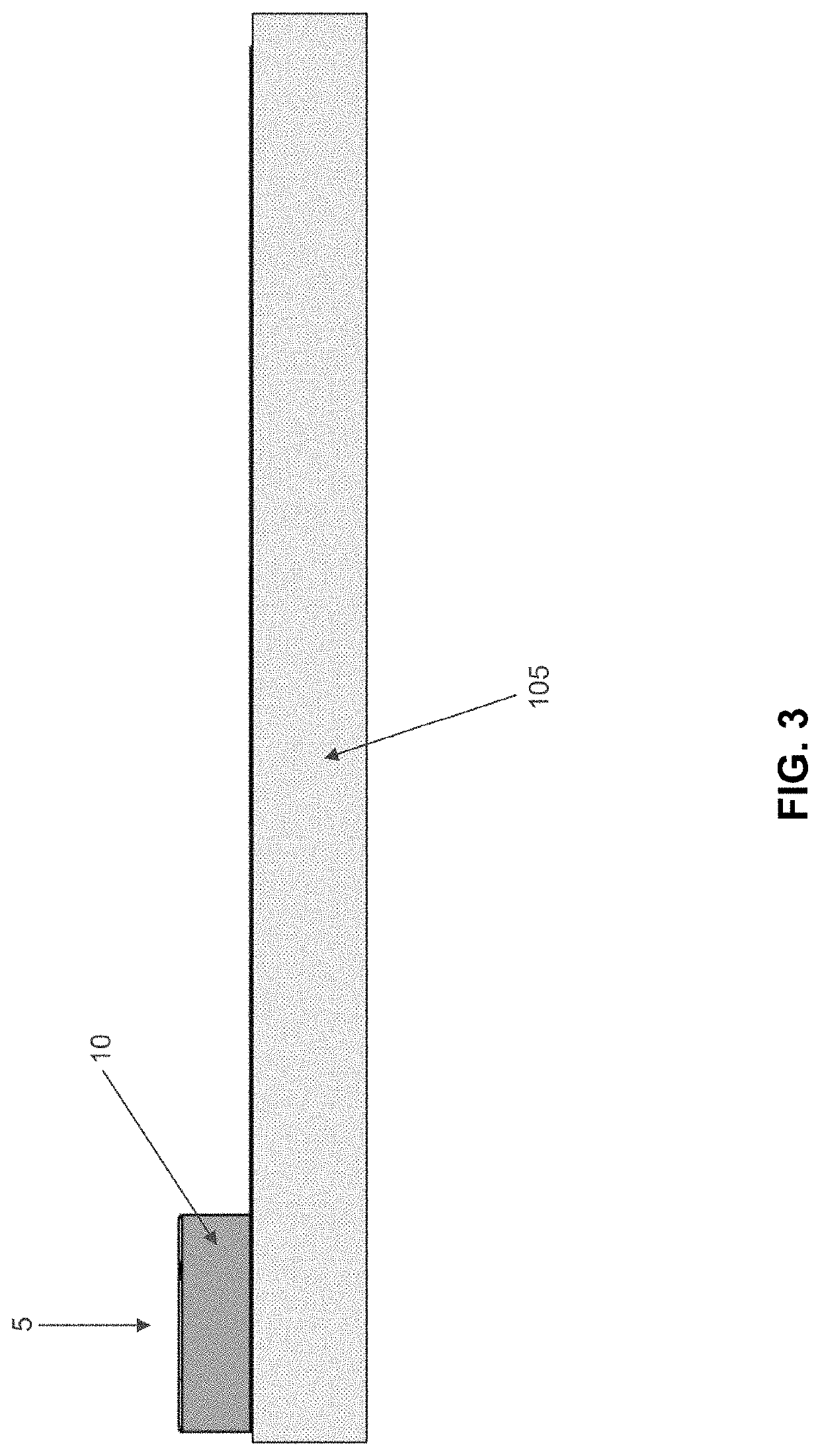
[0054]In one preferred form of the invention, and looking now at FIGS. 1-10, there is provided a widely tunable, single mode emission semiconductor laser 5 which comprises a semiconductor substrate 10 with an epitaxy that allows for semiconductor laser operation, e.g., as a laser diode or as a cascade laser. By way of example but not limitation, semiconductor substrate 10 may comprise a III / V semiconductor material such as gallium nitride (GaN), gallium arsenide (GaAs), indium phosphide (InP) or gallium antimonide (GaSb), depending on the target wavelength range of the laser. The epitaxy generally comprises a layer structure that contains an active zone with one or more quantum films, upper and lower cladding, and upper and lower waveguide layers. More particularly, the widely tunable, single mode emission semiconductor laser 5 has a cuboid shape with the bottom formed by semiconductor substrate 10 and the top formed by an upper waveguide layer which is structured so as to provide t...


PUM


Abstract

The present invention provides a widely tunable, single mode emission semiconductor laser which comprises a semiconductor substrate, a first linear ridge waveguide which forms a first coupled cavity, and a second linear ridge waveguide which forms a second coupled cavity, with the first coupled cavity being separated from the second coupled cavity by a gap. The first and second coupled cavities comprise p-contacts and n-contacts for allowing laser currents I1, I2 to be injected into the first and second coupled cavities, respectively. The first and second coupled cavities comprise first and second heating resistors, respectively, for heating the first and second coupled cavities when heating currents H1, H2 are applied to the first and second heating resistors, respectively. A heating resistor is provided for heating the semiconductor substrate of the semiconductor laser so as to regulate the base temperature T of the chip (i.e., the semiconductor substrate).

Description

REFERENCE TO PENDING PRIOR PATENT APPLICATION[0001]This patent application claims benefit of pending prior U.S. Provisional Patent Application Ser. No. 63 / 004,816, filed Apr. 3, 1920 by Automotive Coalition For Traffic Safety, Inc. and Tim Koslowski et al. for WIDELY TUNABLE, SINGLE MODE EMISSION SEMICONDUCTOR LASER (Attorney's Docket No. ACTS-5 PROV), which patent application is hereby incorporated herein by reference.FIELD OF THE INVENTION[0002]This invention relates to lasers in general, and more particularly to widely tunable, single mode emission semiconductor lasers.BACKGROUND OF THE INVENTION[0003]Single mode emission semiconductor lasers provide light sources for many modern applications, ranging from spectroscopy to telecommunications and far beyond. These single mode emission semiconductor lasers allow for electronic control of the light output and the emitted wavelength A.[0004]For many applications, it is desirable to have a wide tuning range of the laser's emitted wavel...

Claims


Application Information

Patent Timeline
IPC IPC(8): H01S5/22H01S5/026H01S5/042H01S5/024H01S5/065H01S5/02
CPCH01S5/22H01S5/0261H01S5/0206H01S5/02476H01S5/0654H01S5/0422H01S5/1021H01S5/04256H01S5/02453H01S5/0622H01S5/0612H01S5/02315
Inventor KOSLOWSKI, TIMKOETH, JOHANNESKOSLOWSKI, NICOLAS
Owner AUTOMOTIVE COALITION FOR TRAFFIC SAFETY
Why Eureka
Try Eureka