Magnetic tunneling junctions with a magnetic barrier
a magnetic barrier and tunneling junction technology, applied in semiconductor devices, digital storage, instruments, etc., can solve the problems of high power consumption in part, difficult switching of the magnetization direction of the mtjs for writing, and inability to scale up the method,
- Summary
- Abstract
- Description
- Claims
- Application Information
AI Technical Summary
Benefits of technology
Problems solved by technology
Method used
Image
Examples
example
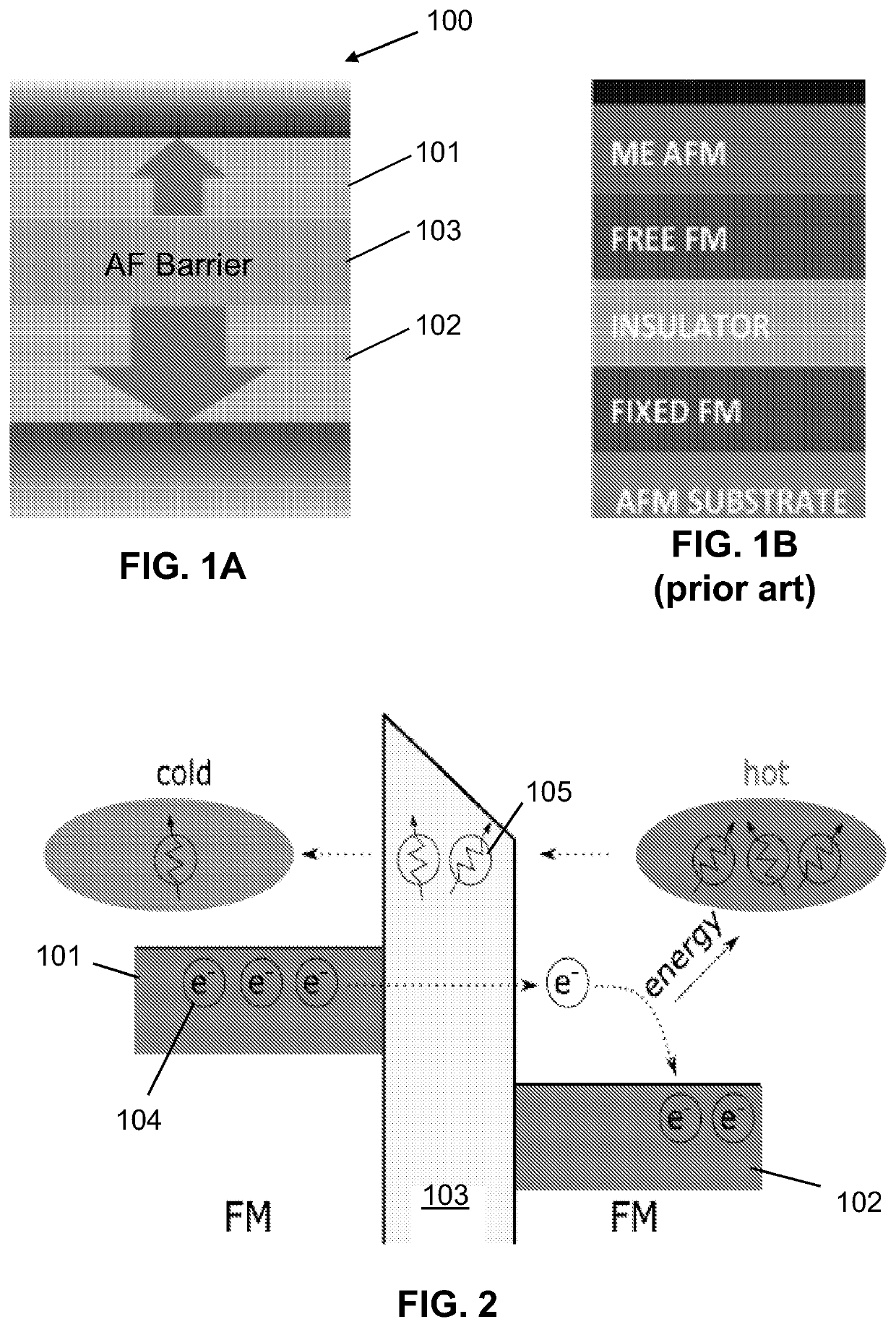
[0051]The following is a non-limiting example of the present invention, specifically, a magnetic tunneling junction with an antiferromagnetic insulator. It is to be understood that said example is not intended to limit the present invention in any way. Equivalents or substitutes are within the scope of the present invention.
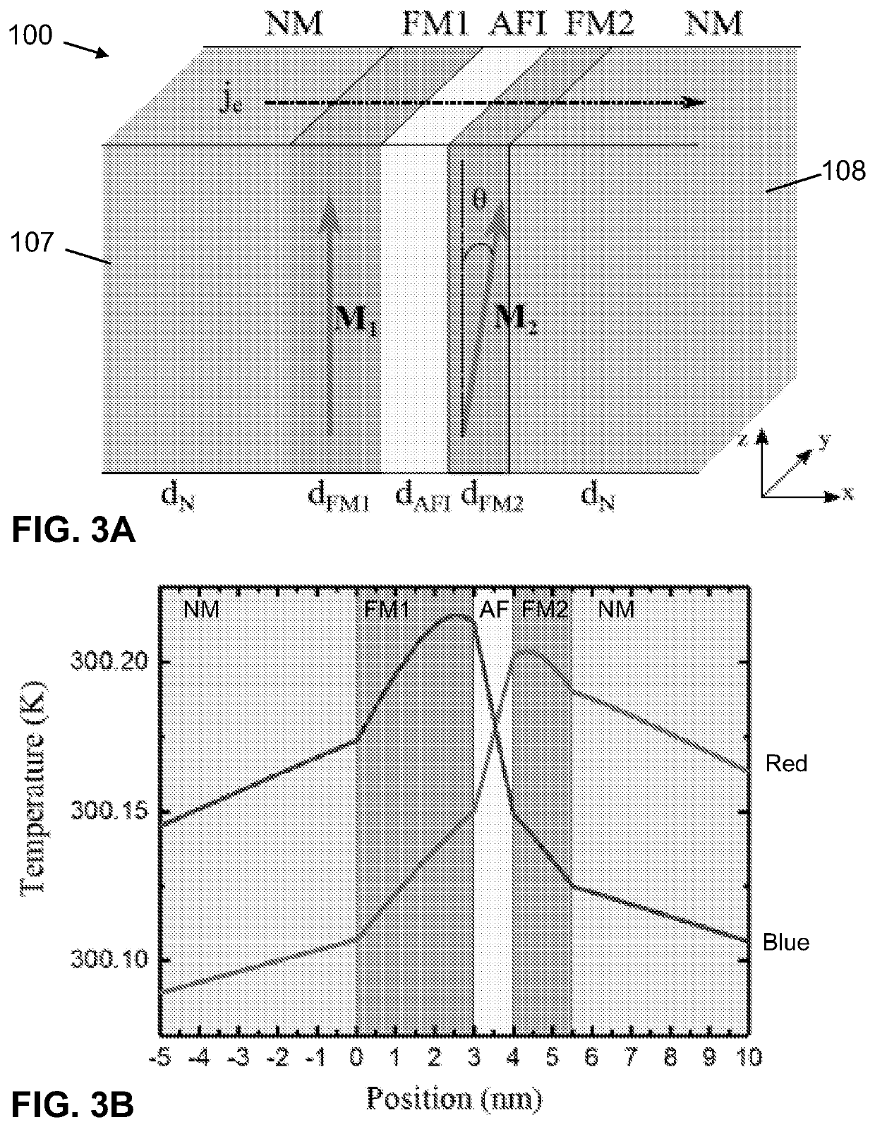
[0052]It is an objective of the invention to provide an MTJ with an AFI replacing MgO as the tunnel barrier for tunnel transport. Consider a tunnel junction made of two FM metals separated by a thin AFI, as shown in FIG. 3A. When a voltage is applied across the tunnel barrier, electrons tunnel from the electrode with the lower voltage to that with the higher voltage. While the tunneling electron will relax its energy in both electrodes, the majority of the energy is relaxed in the electrode receiving the tunnel electron. Since the inelastic mean free path is only a few angstroms for the tunnel electron with the energy about 0.5 eV above the Fermi level, the heat ...
PUM
 Abstract
Description
Claims
Application Information
 - R&D
- Intellectual Property
- Life Sciences
- Materials
- Tech Scout
- Unparalleled Data Quality
- Higher Quality Content
- 60% Fewer Hallucinations
Browse by: Latest US Patents, China's latest patents, Technical Efficacy Thesaurus, Application Domain, Technology Topic, Popular Technical Reports.
© 2025 PatSnap. All rights reserved.Legal|Privacy policy|Modern Slavery Act Transparency Statement|Sitemap|About US| Contact US: help@patsnap.com


