LED device for providing area light source and manufacturing method thereof

a technology of area light source and manufacturing method, which is applied in the direction of semiconductor devices, basic electric elements, electrical appliances, etc., can solve the problems of direct damage to led, shift of wavelength, and reduced lifetime of led, so as to reduce the effect of thermal stress and improve the thermal dissipation performance of a produ

Inactive Publication Date: 2021-02-04
LEDA CREATIVE INC
View PDF0 Cites 3 Cited by
  • Summary
  • Abstract
  • Description
  • Claims
  • Application Information

AI Technical Summary

Benefits of technology

The present disclosure is about an LED device that can provide a bright light to an area. The invention aims to improve the device's ability to handle high temperatures and prevent damage caused by thermal stress. The method for making the LED device is also included. This invention can help to make products that are more durable and reliable.

Problems solved by technology

Considering that a light emitting diode (LED) generates a large amount of heat during operation, and the heat accumulated thereby decreases the brightness of LED, shifts the wavelength, reduces a lifetime of LED, and even directly damages the LED.
In scenarios where a plurality of LEDs are used to provide the area light source, the heat that is generated by the LED increases as the amount of LEDs are increased; furthermore, the shorter the distance between LEDs, the more difficult it is for an accumulated heat to be dissipated.
Therefore, the heat dissipation issue becomes even more difficult to resolve.
In addition to the adverse effects on the LED, the heat has an effect on a substrate bearing the LED.
During the operation of LED for providing the area light source, the heat that is accumulated in the substrate lead to thermal expansion of the substrate, hence, in addition to causing a warpage of the substrate, the accumulated heat affects an interval distance between LEDs.
Under the circumstances, in respect to the substrate for mounting the LED, how a heat dissipation performance of the entire product can be improved, and how the effects of thermal stress on the LED device can be reduced, have become important issues in the related art.

Method used


Image

  • LED device for providing area light source and manufacturing method thereof
  • LED device for providing area light source and manufacturing method thereof
  • LED device for providing area light source and manufacturing method thereof

Examples


first embodiment

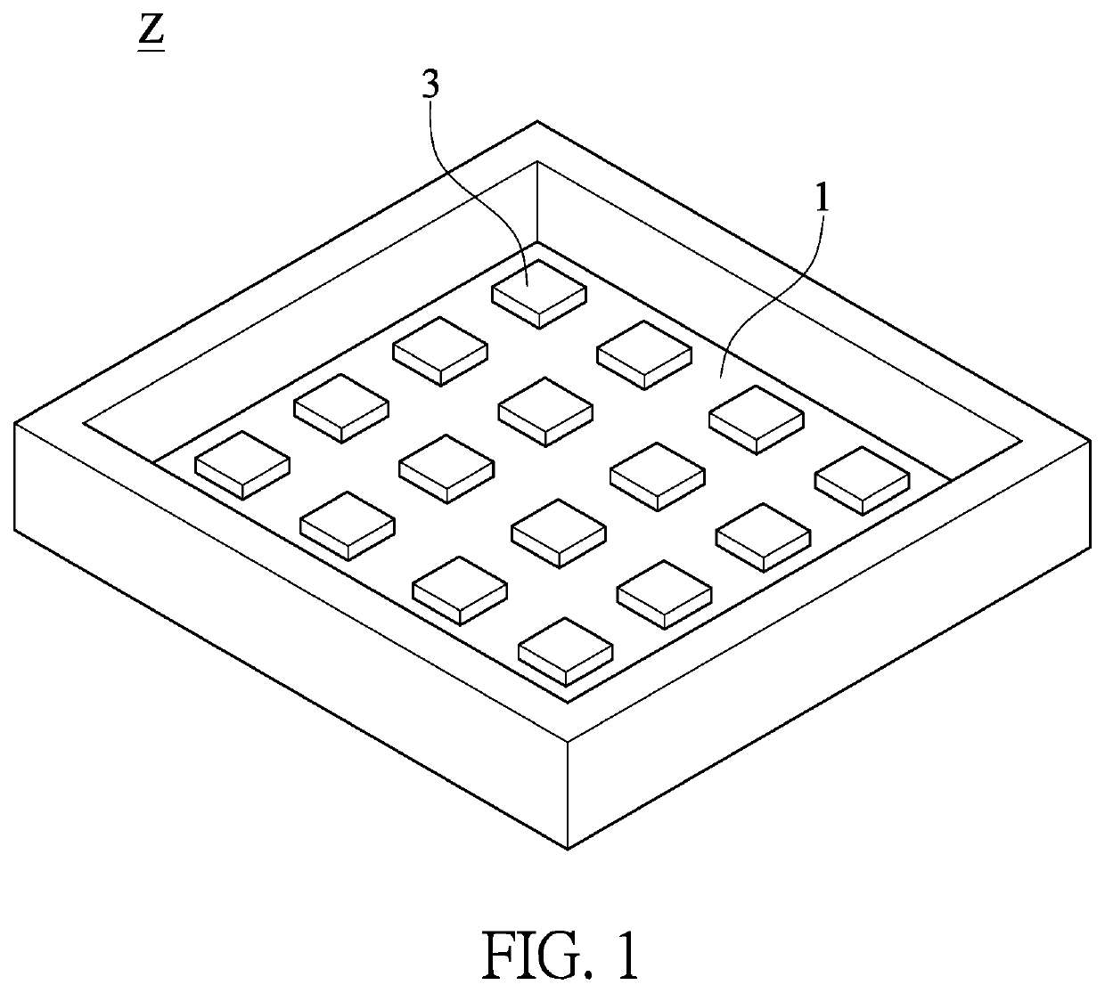
[0025]Referring to FIG. 1 to FIG. 7 and FIG. 11, FIG. 1 is the schematic perspective view of the LED device according to the first embodiment of the present disclosure. FIG. 2 is the schematic partial cross-sectional view of the LED device according to the first embodiment of the present disclosure, wherein the arrangements of one of the LED chips and the substrate are shown. FIG. 3 is the schematic partial upward view of FIG. 2. FIG. 4 is the schematic partial cross-sectional view showing another configuration of the LED device according to the first embodiment of the present disclosure. FIG. 5 is the schematic partial cross-sectional view showing another configuration of the LED device according to the first embodiment of the present disclosure. FIG. 6 is the schematic partial cross-sectional view showing another configuration of an LED device according to the first embodiment of the present disclosure. FIG. 11 is the flow chart of a manufacturing method of LED device according to...

second embodiment

[0045]Referring to FIG. 8 and FIG. 11, FIG. 8 is the schematic partial cross-sectional view of an LED device according to a second embodiment of the present disclosure, wherein a bearing substrate σ and a plurality of excitation materials 7 are further arranged on the top surface of the substrate 1. In contrast to the LED device Z of the first embodiment providing the illumination directly from the light beam that is emitted by the LED chip 3, the LED device Z of the present embodiment provides a first light beam having a first wavelength that is emitted by the LED chip 3, and the first light beam is converted to a second light beam having a second wavelength after the first light beam is projected on the excitation material 7. In other words, the first light beam having the first wavelength emitted by the LED chip 3 is converted to the second light beam having the second wavelength by the excitation material 7. Therefore, the LED device Z of the present embodiment provides the ligh...

third embodiment

[0050]Referring to FIG. 9 and FIG. 11, FIG. 9 is the schematic partial cross-sectional view of the LED device according to a third embodiment of the present disclosure, wherein a sensing element 8 is further arranged on the top surface of the substrate 1. In a particular field of optical detection application (e.g., wearable heart rate measuring device), essentially, the sensing element 8 directly receives a light beam having a particular wavelength that is emitted by a luminous element or a light beam having another wavelength from the reflection from an object. The sensing element 8 then generates a detection signal according to the received results.

[0051]In the present embodiment, in addition to the plurality of LED chips 3 being arranged on the substrate 1 of the LED device Z, a plurality of sensing elements 8 is arranged on the substrate 1 of the LED device Z. The plurality of sensing elements 8 is electrically connected to the metal wiring layer 2 (not shown in the drawings). ...


PUM

PropertyMeasurementUnit
diameteraaaaaaaaaa
diameteraaaaaaaaaa
side lengthaaaaaaaaaa

Abstract

An LED device for providing an area light source and a manufacturing method thereof are disclosed. The LED device for providing the area light source includes a substrate, a metal wiring layer and a plurality of LED chips. The coefficient of thermal expansion of the substrate ranges between 5 and 18 ppm / ° C. on the X-Y direction, and a flexural strength σ ranges between 400 and 600 Mpa according to the ISO 178 test. The metal wiring layer is arranged on a top surface of the substrate. The plurality of LED chips are arranged on the top surface of the substrate for providing the area light source, and a cathode of the LED chips and an anode of the LED chips are separately and electrically connected to the metal wiring layer.

Description

CROSS-REFERENCE TO RELATED PATENT APPLICATION[0001]This application claims the benefit of priority to Taiwan Patent Application No. 108127494, filed on Aug. 2, 2019. The entire content of the above identified application is incorporated herein by reference.[0002]Some references, which may include patents, patent applications and various publications, may be cited and discussed in the description of this disclosure. The citation and / or discussion of such references is provided merely to clarify the description of the present disclosure and is not an admission that any such reference is “prior art” to the disclosure described herein. All references cited and discussed in this specification are incorporated herein by reference in their entireties and to the same extent as if each reference was individually incorporated by reference.FIELD OF THE DISCLOSURE[0003]The present disclosure relates to an LED device and a manufacturing method thereof, and more particularly to the LED device for...

Claims


Application Information

Patent Timeline
Patent Type & Authority Applications(United States)
IPC IPC(8): H01L33/58H01L33/62H01L25/075
CPCH01L33/58H01L33/62H01L2933/0066H01L2933/0058H01L25/0753H01L33/647H01L33/642H01L2933/0075H01L25/167H01L33/54H01L33/507H01L33/505H01L2224/73265H01L2224/48091H01L2924/00014
Inventor HUANG, CHE-HSUANCHANG, SHU-HSIUCHAN, HAO-CHUNGCHUEH, SHAO-CHUN
Owner LEDA CREATIVE INC
Why Eureka
Try Eureka