Solder mask

a technology of soldering mask and soldering cylinder, which is applied in the direction of soldering apparatus, circuit mask, manufacturing tools, etc., can solve the problems of affecting affecting the quality of soldering, so as to improve the reliability of electronic devices, reduce the risk of cracking, and improve the effect of pattern resolution

Active Publication Date: 2020-09-10
PICOSUN OY
View PDF0 Cites 0 Cited by
  • Summary
  • Abstract
  • Description
  • Claims
  • Application Information

AI Technical Summary

Benefits of technology

The present invention provides a method for creating solder mask coatings that are stable at high temperatures required for soldering processes. The method also produces conformal mask coatings to avoid gaps on conductive layers and provide better reliability to electronic devices. The invention also allows for patterning non-planar surfaces and prevents horizontal flow of liquid solder alloys onto undesired areas. The versatility of the method allows for deposition of the mask onto a part of a substrate or the entire substrate.

Problems solved by technology

Creep corrosion has turned out to be a serious problem in the large cities due to the presence of sulfur compounds, such as hydrogen sulfide (H2S), in ambient air.
Creep corrosion annually destroys thousands of circuit boards in server centers, for example, causing damages and losses estimated in several millions USD.
A major drawback associated with the use of organic polymer-based solder masks is that upon soldering, typically at about 250° C., organic material starts to fry, degas and may subsequently melt.
The underlying conductive material becomes exposed to the ambient environment thus becoming more susceptible to corrosion.
Organic vapors released upon subjecting polymer-based mask to high temperatures further cause contamination in soldering area(s); therefore (soldered) components get contaminated, accordingly.
Evaporation of said organic mask material is a major problem in space applications.
Since polymer-based solder masks are typically applied by screen-printing, high lateral patterning resolution and / or deposition of layers less than 1 micrometer thick cannot be attained.
Additionally, organic material is a poor moisture barrier.
Upon diffusing through conventional polymeric solder masks atmospheric moisture causes oxidation and / or corrosion in PCB conductor layer(s) or in the other substrates, thus causing destruction of the PCBs
Exposed conductor areas (copper, silver) are potentially impacted by corrosion.

Method used


Image

  • Solder mask
  • Solder mask
  • Solder mask

Examples


example 2

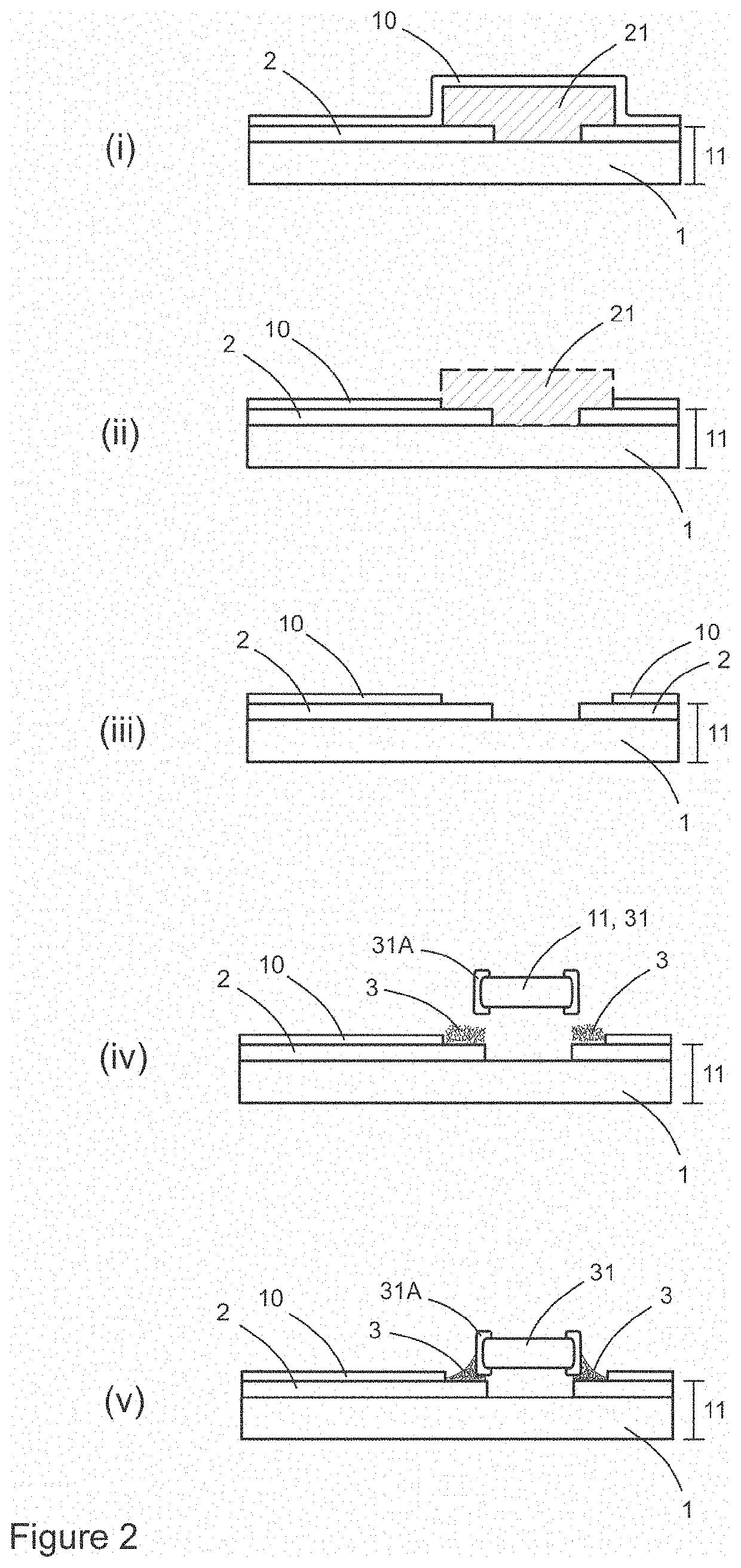
[0059] The mask 10 provided as a layer of titanium dioxide (TiO2) has been deposited on the substrate 11 from titanium tetrachloride (TiCl4) and water. Deposition temperature varies within a range of about 20° C. (room temperature) to about 300° C.

example 3

[0060] The mask 10 provided as a layer of niobium dioxide (Ni2O5) has been deposited on the substrate 11 from niobium ethoxide (Nb2(OC2H5)10) and water. Deposition is possible at least within a range of 90° C. to 150° C.

[0061]In all examples, a layer produced in a single ALD cycle (pulse first precursor—purge; pulse second precursor—purge) has been approximately 0,1 nm. In order to deposit a layer with thickness 10-100 nm, mentioned reactions (cycles) are repeated a predetermined number of times. The deposition procedure may be thus completed within a time range of about 10 minutes to about 20 hours depending on a number of cycles required and duration of each cycle.

[0062]For the purposes of the invention it is preferred that the mask 10 is deposited as a layer having thickness within a range of 10-500 nm, preferably, within a range of 20-200 nm, more preferably, within the range of 50-200 nm, such as 100 nm.

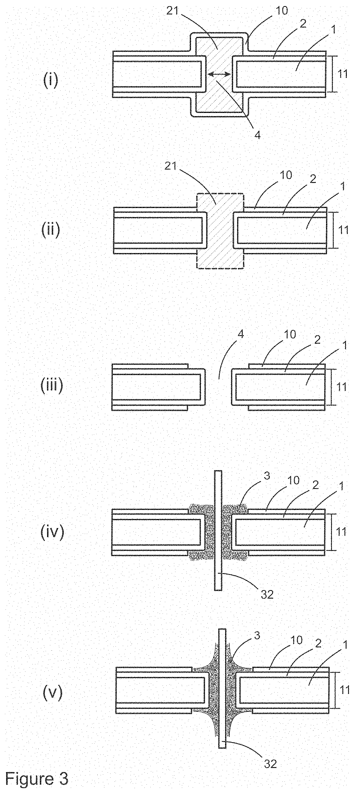
[0063]In similar manner, the mask 10 can be established from three or more ...


PUM

PropertyMeasurementUnit
temperatureaaaaaaaaaa
thicknessaaaaaaaaaa
thickaaaaaaaaaa

Abstract

A method for formation of a patterned solder mask (10) on a substrate is provided, in which method the mask is deposited by a process of chemical deposition in vapor phase. A method for manufacturing a printed circuit board and / or an electronic component comprising formation of said patterned solder mask is further provided.

Description

FIELD OF THE INVENTION[0001]The present invention generally relates to printed circuit boards and electrical components and methods of manufacturing thereof. In particular, the invention pertains to the methods concerning formation of patterned protective layer(s) by chemical vapor deposition.BACKGROUND[0002]Formation of solder mask- or solder resist protective layers on printed circuit boards (PCBs) is generally known in the art. Typical PCB comprises an epoxy substrate laid with a conductive material and further deposited with a layer that prevents solder (e.g. tin solder) wetting at reflow and its' contact to the underlying metal (copper or silver, for example).[0003]Solder mask protects conductive material from corrosion induced by (air) oxidation and / or by the presence of sulfur containing contaminants in ambient air. Creep corrosion has turned out to be a serious problem in the large cities due to the presence of sulfur compounds, such as hydrogen sulfide (H2S), in ambient air...

Claims


Application Information

Patent Timeline
Patent Type & Authority Applications(United States)
IPC IPC(8): H05K3/34B23K1/015
CPCB23K1/015H05K3/3457H05K3/3452B23K2103/50B23K2101/42H05K3/10H05K3/0079H05K1/09H05K2203/0597H05K2203/1338H01L21/0272
Inventor PUDAS, MARKO
Owner PICOSUN OY
Why Eureka
Try Eureka