
Transposable feedback field-effect electronic device and array circuit using the same

Active Publication Date: 2020-03-05
KOREA UNIV RES & BUSINESS FOUND
View PDF5 Cites 4 Cited by
  • Summary
  • Abstract
  • Description
  • Claims
  • Application Information

AI Technical Summary

Benefits of technology

The invention relates to a feedback field-effect electronic device with the following technical effects: bidirectional parallel operation, low power, and high integration. The device can be used as a synapse-imitating device and can improve the degree of integration. It can quickly calculate simultaneous input and output values and reduce power consumption by implementing bidirectional parallel operation. The device can also perform high speed learning and reduce arithmetic delay time by implementing synapse plasticity.

Problems solved by technology

Conventional von Neumann-based computers have a fast operating speed in sequential mathematical calculations, but have limitations in terms of speed and power consumption in calculating simultaneous inputs and outputs.
In the case of conventional memory devices, bidirectional parallel operation may not be performed and implementation of synapse plasticity may be difficult.
However, in fabrication of such memory devices, a conventional complementary metal-oxide-semiconductor (CMOS) process cannot be applied, so that the uniformity and stability of the device may be deteriorated, and the fabrication process is complicated.
However, in the case of 8T-SRAM, eight transistors are included in one memory cell, and an additional circuit is required to implement synapse plasticity, resulting in limitation in the degree of integration.
However, bidirectional parallel operation and synapse plasticity cannot be implemented only by the memory device based on the feedback loop memory mechanism.
In addition, there has been no technology to implement bidirectional parallel operation by connecting an access transistor to the memory device based on the feedback loop memory mechanism.

Method used


Image

  • Transposable feedback field-effect electronic device and array circuit using the same
  • Transposable feedback field-effect electronic device and array circuit using the same
  • Transposable feedback field-effect electronic device and array circuit using the same

Examples


Embodiment Construction

[0049]Hereinafter, various embodiments of the present disclosure will be described with reference to the accompanying drawings.

[0050]It should be understood that embodiments and terminology used herein are not intended to limit the present disclosure, but to include various modifications, equivalents, and / or alternatives of the embodiments.

[0051]In the following description of the present disclosure, detailed description of known functions and configurations incorporated herein will be omitted when it may make the subject matter of the present disclosure unclear.

[0052]The terms used in the specification are defined in consideration of functions used in the present disclosure, and can be changed according to the intent or conventionally used methods of clients, operators, and users. Accordingly, definitions of the terms should be understood on the basis of the entire description of the present specification.

[0053]In description of the drawings, like reference numerals may be used for...


PUM


Abstract

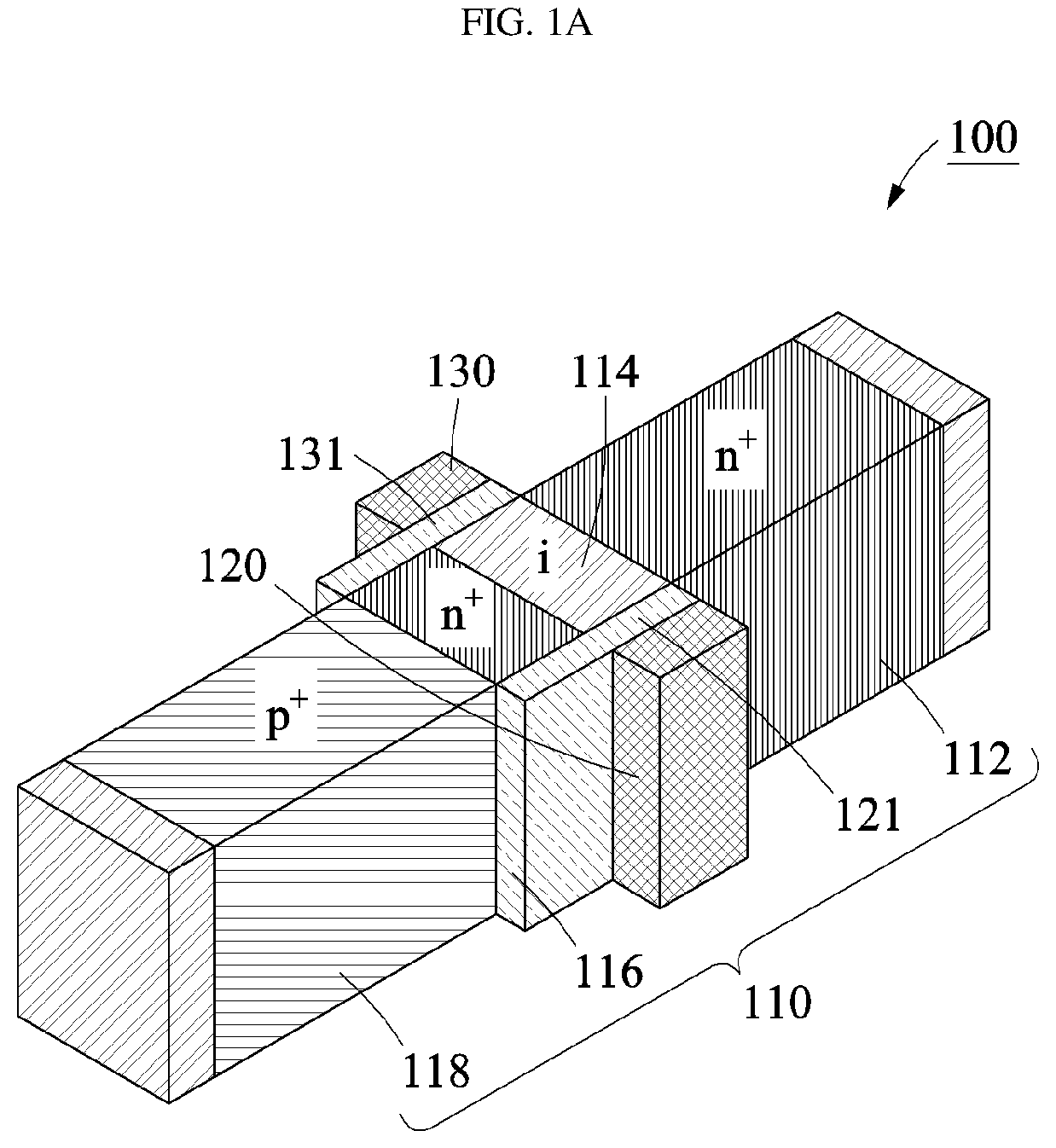
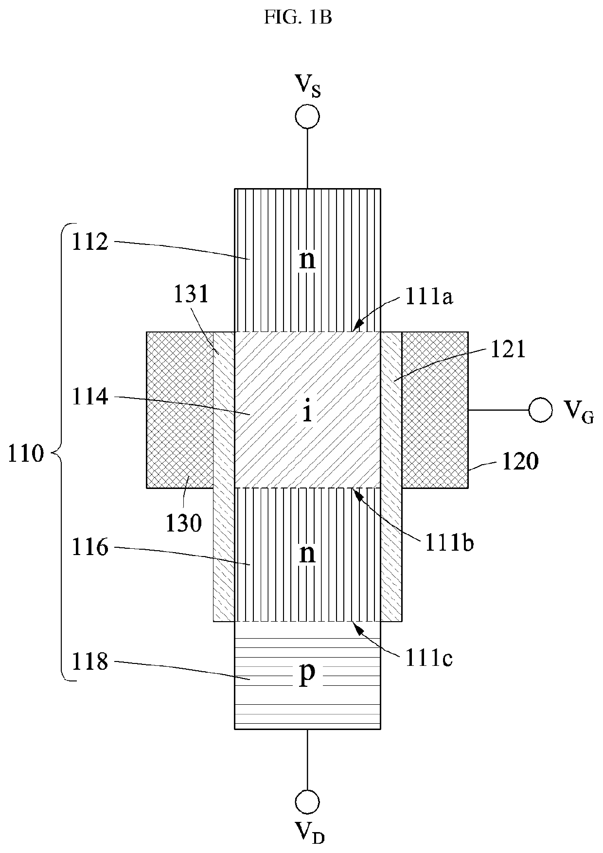
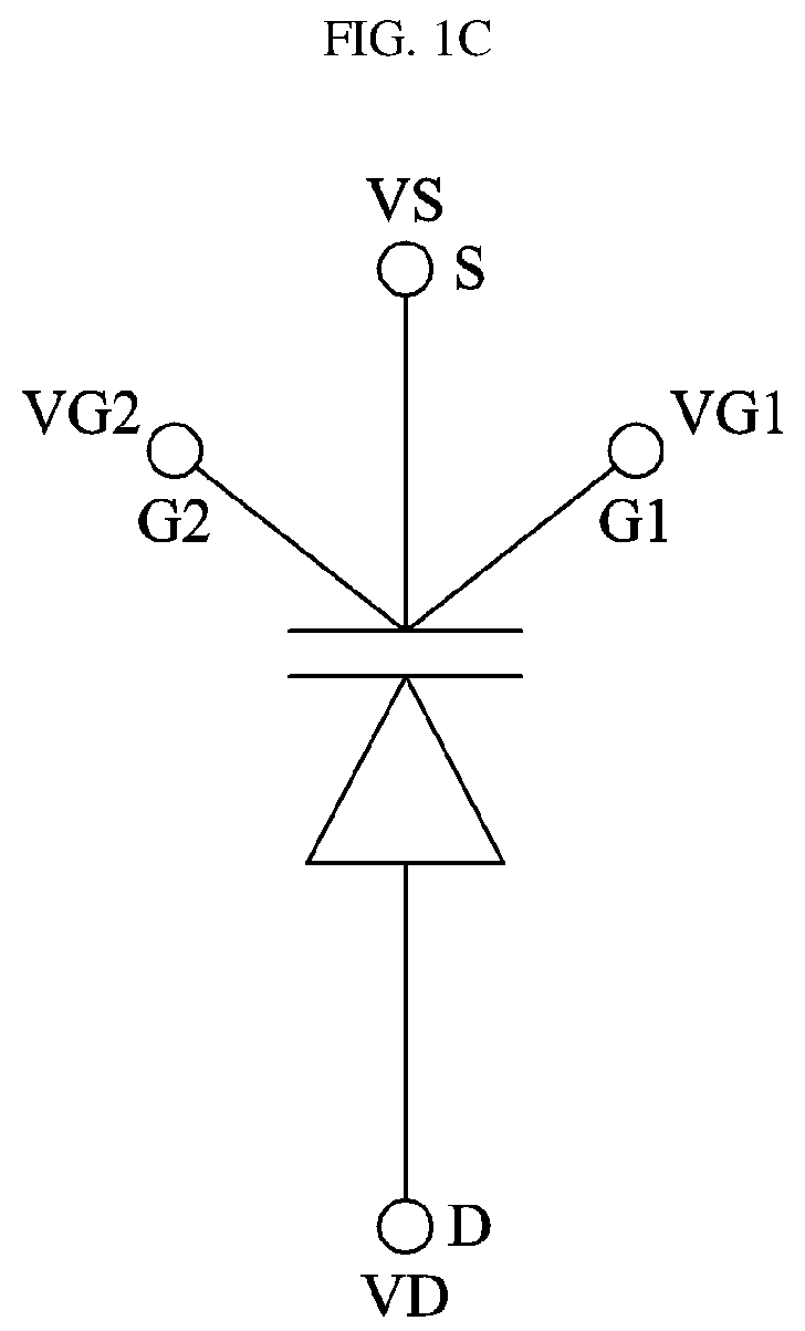
The present disclosure discloses a transposable feedback field-effect electronic device and an array circuit using the feedback field-effect electronic device. According to one embodiment of the present disclosure, the feedback field-effect electronic device may include a diode structure, a plurality of gate electrodes, and a plurality of access electronic devices, wherein, when the diode structure receives voltage through a first gate electrode of the gate electrodes and a first access electronic device of the access electronic devices, first direction access may be performed, and when the diode structure receives voltage through a second gate electrode of the gate electrodes and a second access electronic device of the access electronic devices, second direction access may be performed.

Description

CROSS-REFERENCE TO RELATED APPLICATION[0001]This application claims priority to Korean Patent Application No. 10-2018-0106112, filed on Sep. 5, 2018 in the Korean Intellectual Property Office, the disclosure of which is incorporated herein by reference.BACKGROUND OF THE DISCLOSUREField of the Disclosure[0002]The present disclosure relates to a feedback field-effect electronic device that is transposable and is usable as a synapse array device. More specifically, the present disclosure relates to a transposable feedback field-effect electronic device capable of controlling row-direction access and column-direction access by connecting two access transistors to a feedback field-effect transistor using two independent gate electrodes, and relates to an array circuit using the feedback field-effect electronic device.Description of the Related Art[0003]Neuromorphic technology is a technology that imitates human nerve structures using electronic devices and circuits.[0004]Conventional von...

Claims


Application Information

Patent Timeline
IPC IPC(8): G11C11/54G11C11/412H01L29/739H01L27/105G11C11/419
CPCG11C11/412H01L29/7391G11C11/54G11C11/419H01L27/1052H01L27/0629G06N3/063G11C11/36G11C8/16H01L29/42312H10B99/00H01L27/0611H01L21/8238H01L27/105H01L27/092
Inventor KIM, SANG SIGCHO, KYOUNG AHCHO, JIN SUNLIM, DOO HYEOKWOO, SOL A
Owner KOREA UNIV RES & BUSINESS FOUND
Learn More