
Inductively doped mixed layers for an optoelectronic component, and method for the production thereof

a technology of optoelectronic components and mixed layers, which is applied in the field of optoelectronic components, can solve the problems of natural limitation, poor electrical performance of organic semiconductors, and disadvantages of current use of organic semiconductors, so as to save time, material and work steps, and prolong the useful li

Active Publication Date: 2020-01-16
INURU GMBH
View PDF3 Cites 1 Cited by
  • Summary
  • Abstract
  • Description
  • Claims
  • Application Information

AI Technical Summary

Benefits of technology

The modified method described in the patent produces a reliable and strong component. It involves steps of printing electroactive or optically active layers onto a cathode using a printing method. A second layer, such as an electron transport layer, can be added to form a mixed layer that improves the performance of the component. The resulting component is high-performing and can be used for light generation. This method provides a simple and effective way to produce reliable and strong components.

Problems solved by technology

However, in comparison to organic semiconductors, the currently used organic semiconductors have disadvantages.
Thus, the electrical performance of the organic semiconductors, i.e., in particular the conductivity, is on average poorer than that of conventional inorganic semiconductors.
This results in a natural limitation.
This limitation manifests itself as a limiting factor for the electrical conductivity of the organic systems.
However, the disadvantage of the methods is the high process costs.
On the one hand, expensive installations are necessary for the vacuum deposition.
Moreover, the methods are characterized by a high material loss, since the deposition as a rule occurs nonspecifically and the deposition occurs not only on the substrate but also on other parts of the vaporization installations.
While, in the spin coating or dip coating methods, doped organic semiconductors can also be applied, this is not possible on the industrial scale in the common printing methods.
By the doping of the organic semiconductors, aggregates form in the solution, which prevent an effective printing or at least impede it considerably.
Here clogging occurs in the printing heads.
Thus, at this time, there are no suitable printing methods in industry for the reliable and cost-effective production of organic optoelectronic component parts with printing of p- or n-doped organic materials.
Another disadvantage of known printing methods for organic semiconductor layers manifests itself in the production of thin layer component parts having complex, multi-layered structures with 3-8 layers, for example.
Such uncontrolled superficial dissolution could otherwise lead to defects or damage of the layers, thereby considerably reducing the electrical performance as well as the useful life of the optoelectronic component part.
Typical temperatures for cros slinking are 150-250° C., while normal drying of the wet layer occurs at 100-140° C. In addition, the crosslinking method tends rather to damage the organic materials (degradation temperatures of the organic materials are in the range of 140-250° C.) and is limited in use to only to a few highly stable organic materials.
Moreover, processing in air is also no longer possible, since the organic materials below their intrinsic decomposition temperatures start to oxidize with oxygen.
However, a disadvantage here is that the initiated chemical reaction for crosslinking the organic material has a negative influence on the electrical performance, in particular due to a decrease of the charge carrier mobility.
For example, the pi systems responsible for the charge transport often are impaired or destroyed.
Typical temperatures for the crosslinking are 150-250° C., while the normal drying of the wet layer occurs at 100-140° C. From this, it results that the crosslinking method tends to damage the organic materials.
Moreover, processing in air is not possible, since the organic materials below their intrinsic decomposition temperatures start to oxidize with oxygen.
However, it is precisely in thin layer structures with more than 3 layers that this condition rapidly leads to difficulties in the practical implementation.
The hybrid methods are clearly more expensive and cost-intensive than a complete printing of the layers, due to the necessity of the additional vapor deposition steps.

Method used


Image

  • Inductively doped mixed layers for an optoelectronic component, and method for the production thereof
  • Inductively doped mixed layers for an optoelectronic component, and method for the production thereof
  • Inductively doped mixed layers for an optoelectronic component, and method for the production thereof

Examples


example 1

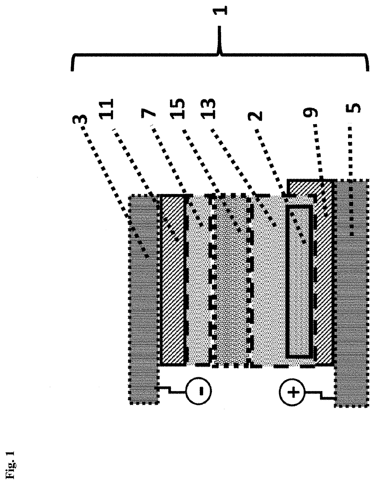
[0166]FIG. 1 shows a diagrammatic representation of a preferred embodiment of the optoelectronic component 1 with an inductively doped mixed layer. The optoelectronic component 1 represented is an organic light emitting diode (OLED). The layer structure of same has the following composition. A cathode 3 is used for providing electrons, while the anode 5 supplies electron holes, as soon as a voltage is applied to them. The signs + and − indicate the respective voltage direction. The properties of the electron injection layer 7 and of the hole injection layer 9 preferably enable an efficient quantum mechanical tunneling of the charge carriers. The electron transport layer 11 and the hole transport layer 13 are characterized by a high mobility for the charge carriers and ensure a targeted transport toward the optically active layer 15 which is a light generating or emitter layer. In the optically active layer 15, the charge carriers recombine, with generation of excitons and the radiat...

example 2

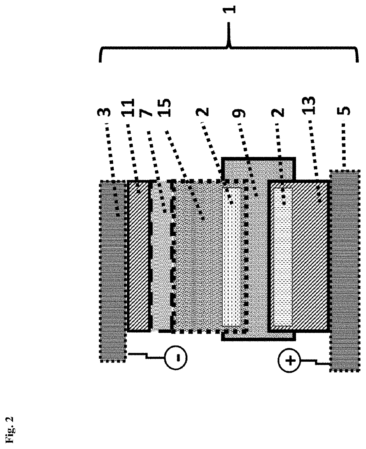
[0179]FIG. 2 shows a diagrammatic representation of an additional preferred embodiment of an optoelectronic component 1 with two inductively doped mixed layers 2. As in the case of FIG. 1, the optoelectronic component 1 represented is an organic light emitting diode (OLED). The function of the individual layers of the layer structure is analogous to FIG. 1.

[0180]However, the OLED represented is characterized in that both between a hole transport layer 13 and a hole injection layer 9 and also between the hole injection layer 9 and the optically active layer 15 an inductively doped mixed layer 2 is present in each case.

[0181]The inductively doped mixed layers result from successive application of the layers 13, 9 and 15 with the help of a printing method with suitable selection of the carrier means of the printing inks. In the process, in particular the carrier means of the printing ink for the second hole injection layer 9 to be applied is selected in such a manner that it can superf...


PUM

PropertyMeasurementUnit
Temperatureaaaaaaaaaa

Abstract

An optoelectronic component with a cathode and an anode and a layer system between the cathode and the anode is provided. The optoelectronic component having multiple electroactive layers, wherein the component can be produced by a method in which an inductively doped mixed layer is generated between at least two layers made of semiconductor materials.

Description

[0001]The invention preferably relates to an optoelectronic component with a cathode and an anode and with a layer system between the cathode and the anode, comprising multiple electroactive layers, wherein the component can be produced by a method in which an inductively doped mixed layer is generated between at least two layers made of semiconductor materials.PRIOR ART AND BACKGROUND[0002]The invention relates to the field of optoelectronic components. Optoelectronic components, for example, on an organic base, or in the form of hybrid components made of organic and inorganic layers, are commonly used in the technology.[0003]Organic light emitting diodes (OLEDs) consist generally of a sandwich structure, wherein multiple layers of organic semiconductor materials are generally located between two electrodes. In particular, an OLED comprises one or more emitter layers (EL) in which electromagnetic radiation, preferably in the visible range, is generated by a recombination of electro...

Claims


Application Information

Patent Timeline
IPC IPC(8): H01L51/50H01L51/00H10K99/00
CPCH01L51/0043H01L51/5056H01L51/0004H01L51/5092H01L51/5076H01L51/5008Y02E10/549Y02P70/50H10K71/13H10K30/865H10K71/00H10K50/15H10K50/165H10K50/171H10K85/151
Inventor BARKOWSKI, PATRICKRATAJCZAK, MARCIN
Owner INURU GMBH
Learn More