
Sige source/drain structure and preparation method thereof

Active Publication Date: 2018-06-07
SHANGHAI HUALI MICROELECTRONICS CORP
View PDF2 Cites 0 Cited by
  • Summary
  • Abstract
  • Description
  • Claims
  • Application Information

AI Technical Summary

Benefits of technology

This patent provides a structure and method for preparing SiGe source / drain to improve its epitaxy in an incomplete un-tuck structure. It includes adding a lattice change layer which increases the growth of SiGe and avoids the infiltration of NiSi into the substrate, improving the morphology of the top layer and preventing the issues of abnormal resistance and leakage of active area. The added layer also promotes the growth of the cap layer and enhances the thickness and uniformity of SiGe in the structure. Overall, this invention helps to improve the quality of SiGe source / drain and prevent issues during semiconductor device manufacturing.

Problems solved by technology

Since the semiconductor manufacturing technology has been developed into the nano-scale, scaling down technology is facing more and more serious challenges.
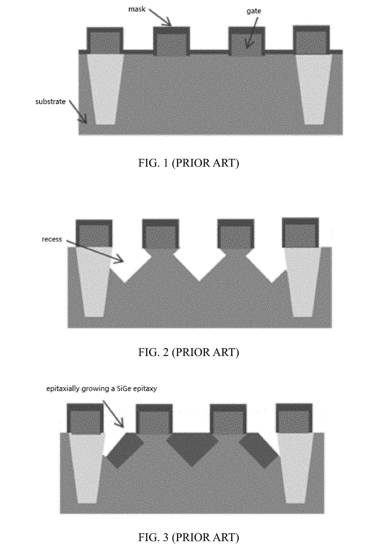
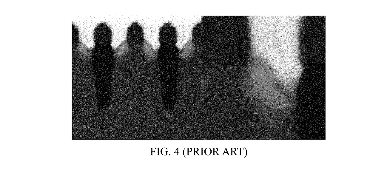
Specifically, in the embedded SiGe technology, due to epitaxial growth has crystal orientation selectivity (such as, epitaxial growth is the fastest in the crystal orientation, faster in the crystal orientation, and almost impossible in the crystal orientation), the crystal plane of the SiGe epitaxy in the un-tuck structure more easily formed at the area near the STI structure will restrain the growth of the SiGe seed layer and the SiGe bulk layer, so cause the insufficient of thickness of the SiGe seed layer and the SiGe bulk layer, as shown in the FIG. 3.
In other words, the thickness of the cap layer grown on the crystal plane is insufficient.
It is well known by the person skilled in the art that, in the subsequent metal silicide reaction, Ni atom is easy to infiltrate into the bottom semiconductor single crystal silicon substrate, so that lead to the leakage of the active area.
In addition, SiGe epitaxy with high germanium concentration is difficult to react with Ni to form metal silicide (NiSi or NiGeSi), so that cause poor contact between subsequent contact hole and the SiGe epitaxy, and further cause leakage, increased resistance and uncontrolled resistance, and so on.

Method used


Image

  • Sige source/drain structure and preparation method thereof
  • Sige source/drain structure and preparation method thereof
  • Sige source/drain structure and preparation method thereof

Examples


Embodiment Construction

[0050]The present invention will be described in further details hereinafter by referring to the accompanying drawings, so as to provide a better understanding of the present invention.

[0051]It should be noted that, in the following specific embodiments, when these embodiments of the present invention are described in detail, in order to clearly illustrate the structure of the present invention to facilitate explanation, the accompanying drawings are not necessarily drawn to scale, some features in the drawings may have been fragmentary enlarged, deformed or simplified. Therefore, it should be avoided to understand this as a limitation to the present invention.

[0052]Compared with the prior art, the same with the prior art, structure of SiGe source / drain of the present invention comprises a semiconductor single crystal silicon substrate, a SiGe seed layer and a SiGe bulk layer, and a cap layer. Wherein, the semiconductor single crystal silicon substrate has a prepared gate and two re...


PUM


Abstract

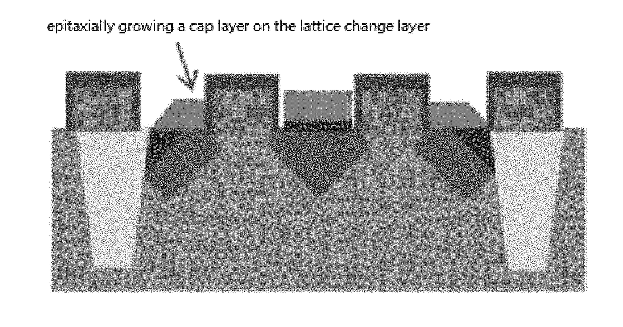
A structure of SiGe source / drain and a preparation method thereof are disclosed in the present invention. Firstly, providing a semiconductor single crystal silicon substrate. Secondly, etching the semiconductor single crystal silicon substrate to form recesses on both sides of the gate. Thirdly, epitaxially growing a SiGe seed layer and a SiGe bulk layer in the recesses in turn. Fourthly, subjecting the SiGe bulk layer to a crystal plane treatment with a mixed-gases. Fifthly, epitaxially growing a lattice change layer on the SiGe bulk layer. Finally, epitaxially growing a cap layer on the lattice change layer. The preparation method of the present invention can greatly improve the morphology of the SiGe epitaxy in the incomplete Un-tuck structure, and promote the formation of the subsequent metal silicide (NiSi), so that problems such as abnormal resistance and leakage of active area (AA leakage) can be effectively prevented.

Description

CROSS-REFERENCE TO RELATED APPLICATION[0001]This application claims the priority benefit of China patent application serial No. 201611093086.2, filed Dec. 1, 2016. The entire contents of the above-mentioned patent application are hereby incorporated by reference herein and made a part of the specifications.FIELD OF THE INVENTION[0002]The present invention relates to semiconductor silicon wafer process in the field of IC manufacturing technology, and particularly to a structure and preparation of SiGe source / drain.BACKGROUND OF THE INVENTION[0003]With the development of the IC manufacturing technology, the size of field effect transistor (FET) has been reducing. So, strain technology has been introduced to change lattice structure of channel for improving the carrier mobility in a channel. It has been known from the existing studies that the application of tensile stress in the channel can increase the electron mobility, while the application of compressive stress can increase the ho...

Claims


Application Information

Patent Timeline
IPC IPC(8): H01L29/78H01L29/165H01L21/8234H01L29/04H01L29/06H01L29/40H01L21/02H01L21/306
CPCH01L29/7848H01L29/165H01L21/823418H01L29/045H01L21/30604H01L29/401H01L21/02532H01L21/0245H01L29/0653H01L29/0847H01L29/66477H01L21/02381H01L21/02579H01L21/0262
Inventor HUANG, QIUMINGTAN, JUNYAN, QIANG
Owner SHANGHAI HUALI MICROELECTRONICS CORP
Learn More