Mother ceramic substrate, ceramic substrate, mother module component, module component, and method of manufacturing mother ceramic substrate
a technology of ceramic substrates and mother ceramics, applied in the direction of printed circuit manufacturing, printed circuit non-printed electric components association, printed circuit aspects, etc., can solve the problems of serious defects, defective appearance and dimensions of individual ceramic substrates obtained by division, and exposure of inner electrodes, etc., to achieve high form accuracy
- Summary
- Abstract
- Description
- Claims
- Application Information
AI Technical Summary
Benefits of technology
Problems solved by technology
Method used
Image
Examples
first embodiment
[0084]In a first embodiment, a method of manufacturing a ceramic substrate (a ferrite substrate) using magnetic ceramic as a ceramic material is described.
[0085](1) First, magnetic ceramic powder (in this first embodiment, ferrite powder), binder resin, and an organic solvent were mixed, molten, dispersed, then deaerated, and thus ceramic raw material slurry was fabricated.
[0086]Then, the ceramic raw material slurry was formed in a sheet shape by a known method such as a doctor blade method, and dried. Thus, a mother ceramic green sheet with a thickness of 200 μm was fabricated.
[0087]The mother ceramic green sheet may be a multilayer body in which a plurality of ceramic green sheets are laminated.
[0088]Then, the obtained mother ceramic green sheet was cut to have a predetermined size, and hence a cut mother ceramic green sheet, being an unfired mother ceramic substrate according to the present disclosure, was obtained.
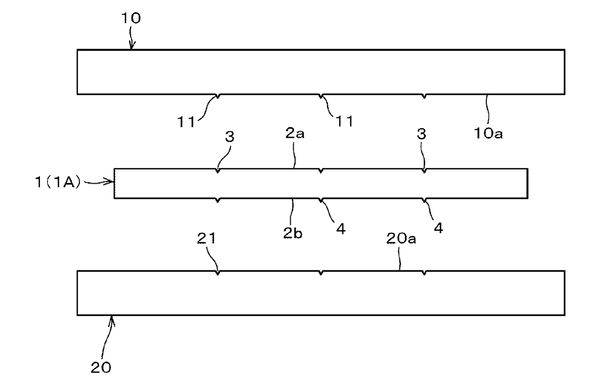
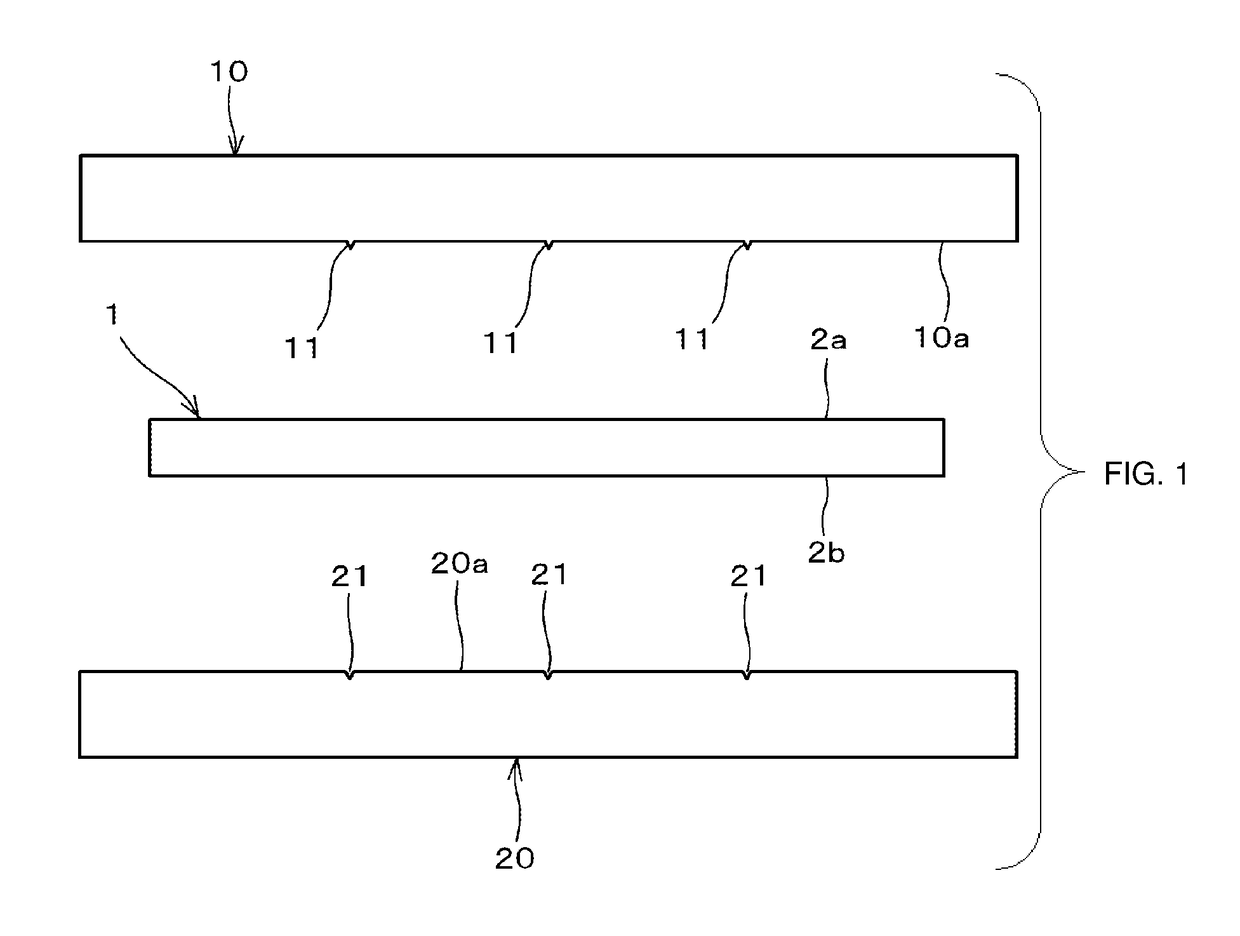
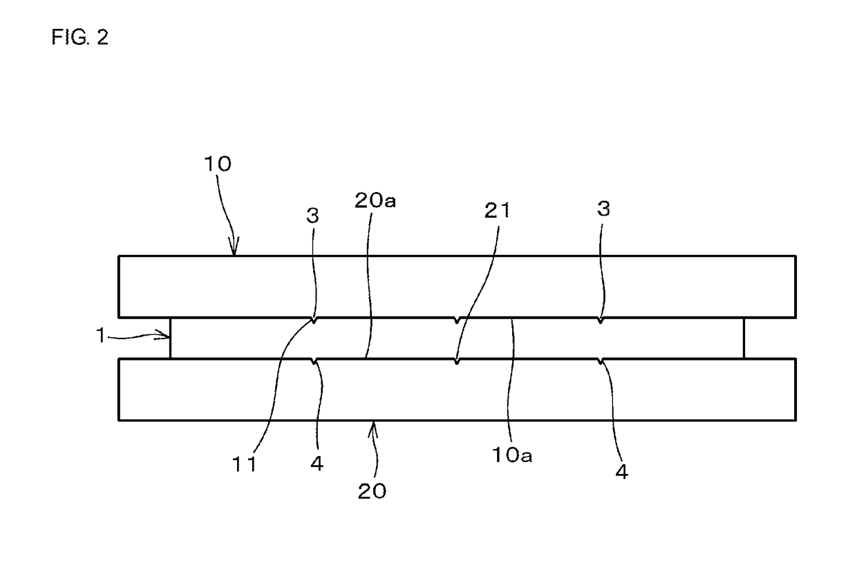
[0089](2) Then, as shown in FIG. 1, a mother ceramic green sheet ...
second embodiment
[0105]In a second embodiment, a method of manufacturing a ceramic substrate (a multilayer ceramic substrate) using low-temperature sintered ceramic as a ceramic material is described.
[0106](1) First, glass ceramic powder (low-temperature sintered ceramic powder), binder resin, and an organic solvent were mixed, molten, dispersed, then deaerated, and thus ceramic raw material slurry was fabricated.
[0107]Then, the ceramic raw material slurry was formed in a sheet shape by a known method such as a doctor blade method, and dried. Thus, a plurality of mother ceramic green sheets each of which has a thickness of 50 μm were fabricated.
[0108]Then, the obtained mother ceramic green sheets were cut to have a predetermined size, a conductive paste (an Ag paste) for forming an inner electrode was applied to each of the mother ceramic green sheets by screen printing, and hence an inner electrode pattern was formed.
[0109]The mother ceramic green sheets may include a via conductor (a kind of inner...
third embodiment
[0115]In a third embodiment, as shown in FIG. 10, a method of manufacturing a module component 150 on which surface mount devices 151 are mounted on a ceramic substrate (a multilayer ceramic substrate) 1 including, for example, a surface conductor, an inner conductor, and a via conductor, is described.
[0116](1) First, a ceramic green sheet (a low-temperature sintered ceramic green sheet) 1 was fabricated by a method similar to that of the second embodiment. Conductive patterns serving as, for example, a surface conductor and an inner conductor were formed and a via hole was formed in the obtained ceramic green sheet 1. The via hole was filled with a conductive material to be a via conductor. Thus, pattern forming sheets 101a each including required conductive patterns 140 were fabricated as shown in FIG. 11.
[0117](2) Then, the pattern forming sheets 101a including the conductive patterns 140 were laminated in a predetermined order (FIG. 12). The obtained multilayer body was put in a...
PUM
| Property | Measurement | Unit |
|---|---|---|
| thickness | aaaaa | aaaaa |
| width | aaaaa | aaaaa |
| height | aaaaa | aaaaa |
Abstract
Description
Claims
Application Information
 - R&D
- Intellectual Property
- Life Sciences
- Materials
- Tech Scout
- Unparalleled Data Quality
- Higher Quality Content
- 60% Fewer Hallucinations
Browse by: Latest US Patents, China's latest patents, Technical Efficacy Thesaurus, Application Domain, Technology Topic, Popular Technical Reports.
© 2025 PatSnap. All rights reserved.Legal|Privacy policy|Modern Slavery Act Transparency Statement|Sitemap|About US| Contact US: help@patsnap.com


