
Method for manufacturing a double-sided printed circuit board

Inactive Publication Date: 2016-09-08
OBSHCHESTVO S OGRANICHENNOJ OTVETSTVENNOSTJU KOMPANIJA RMT
View PDF14 Cites 8 Cited by
  • Summary
  • Abstract
  • Description
  • Claims
  • Application Information

AI Technical Summary

Benefits of technology

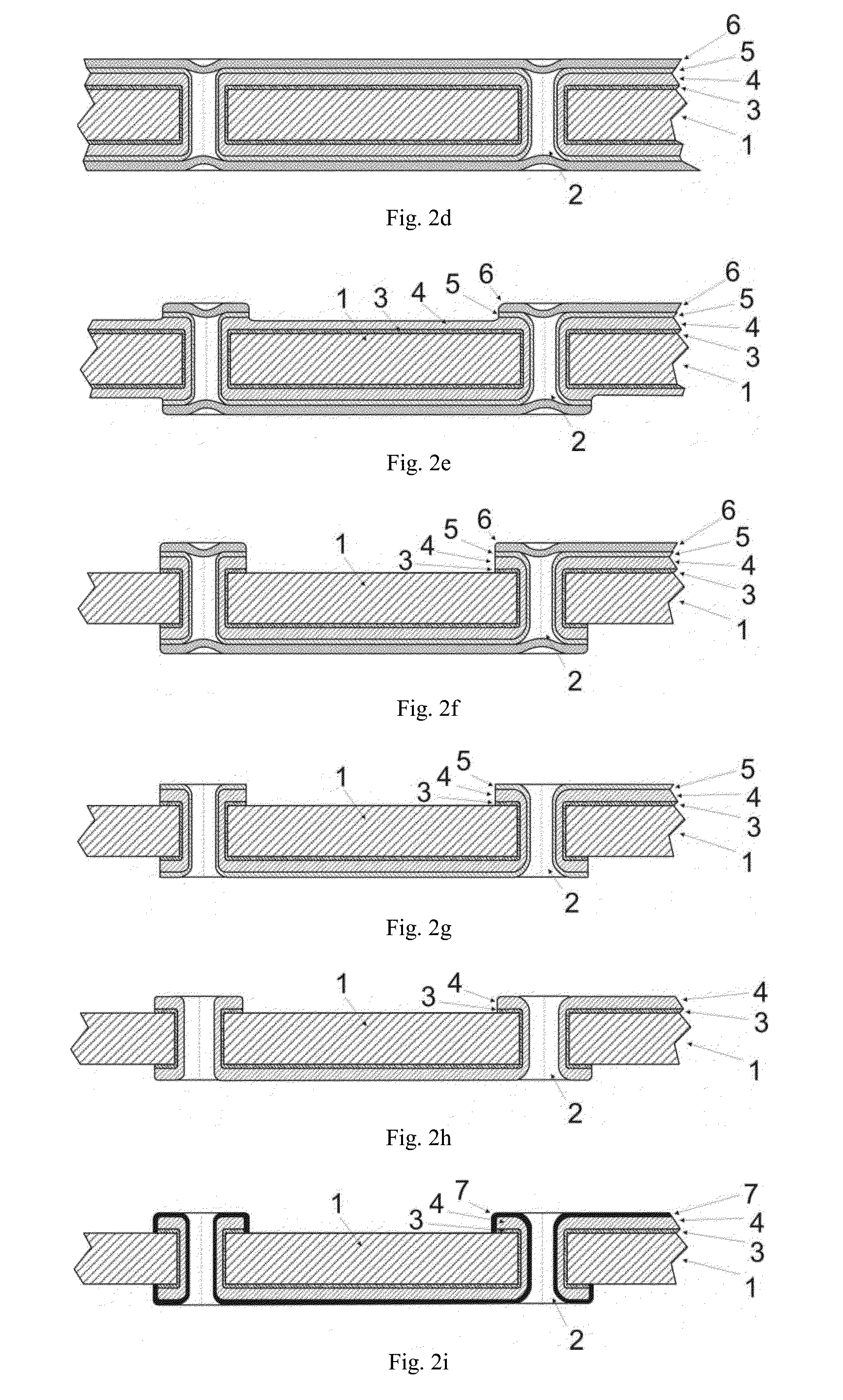
This invention is about a method for making double-sided printed circuit boards. The method includes steps to create vias in a non-conductive substrate, deposit layers onto the substrate and the vias, apply a soluble protective layer, and create a pattern through laser evaporation. The invention results in improved quality and reliability of the metallization pattern, better electrical properties of the conductive layer, and higher efficiency of the manufacturing process.

Problems solved by technology

Drawbacks of these methods comprising surface activation, in spite of their technological simplicity, are their high cost due to the use of activators produced from precious metals as well as insufficiently high adhesion of chemically deposited copper layers to the surface of a polymer array.
However, a drawback of this method is a complex multi-stage process requiring a big volume of precision and expensive equipment.
Moreover, the use of galvanic building-up leads to shortcomings in metallization pattern, i.e., a conductive layer material is loose and of inferior quality in comparison with a voluminous one; the surface is rougher; undercuts are present; etc.
1) The method is a complex and multi-stage one, since it comprises both application of thin metal layers and subsequent galvanic “building-up” of the conductive layer thickness to a value required for good conductance.
2) The conductive layer is a galvanically built-up layer. Layers, which are produced by galvanic building-up, have a loose, as compared to a voluminous material (e.g., copper), structure, and, due to this fact, conduction properties of a galvanic layer are less than those of a voluminous, or even deposited, e.g. by magnetron deposition, material.
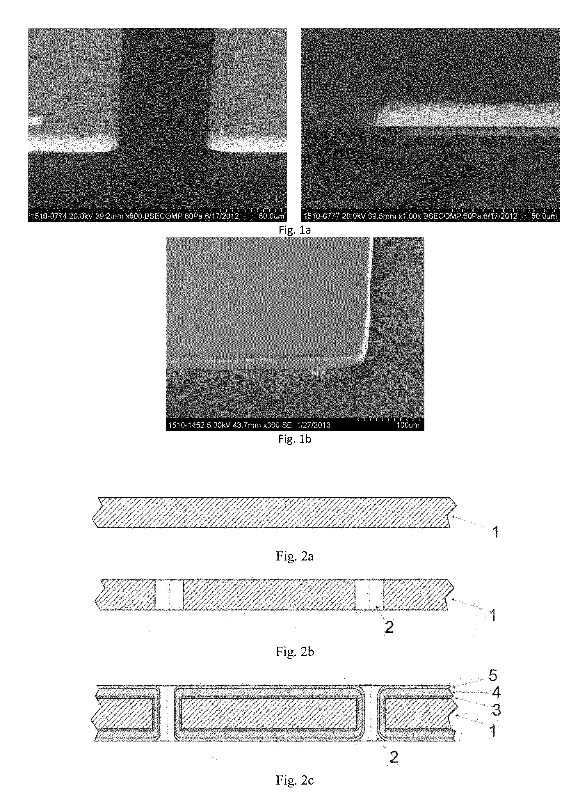
3) At the final stage of this method, when a thin conductive coating is etched, undercutting of the basis of conductive traces occurs, and a cross-section of a conductive trace produced by this technology always looks as that shown in FIG. 1a. Apart from this defect, internal metallization layers of such a trace on the undercut side remain exposed, and such a spot is a place susceptible to future oxidation and corrosion.
4) Moreover, the surface of a layer built-up galvanically has greater roughness (FIG. 1a).

Method used


Image

  • Method for manufacturing a double-sided printed circuit board
  • Method for manufacturing a double-sided printed circuit board
  • Method for manufacturing a double-sided printed circuit board

Examples


examples of specific embodiments

OF THE CLAIMED METHOD

example 1

[0070]A series of vias are produced by laser drilling according to PCB given coordinates in a polished (Ra<0.1) ceramic substrate made of aluminum oxide. The characteristics of laser radiation and produced vias are indicated in Table 1.

TABLE 1Characteristics of laser radiation and vias made therebyPulseRadiationPulserepetitionAverageLaser typewavelengthdurationratepowerVia sizeFiber laser1.064 microns1 μs100 Hz100 W0.25 mm

[0071]Then the multi-layer metal coating, which consists of the adhesion coating, the conductive layer, and the mask layer, is magnetron-deposited onto the substrate with the vias produced. The characteristics of the deposited layers are given in Table 2. Deposition of the multi-layer coating in a single process is performed in a magnetron unit having a corresponding set of magnetron targets (Cr, Cu, V).

[0072]Magnetron deposition is carried out on both sides of the substrate and in the vias.

TABLE 2Composition and parameters of the metallization layers depositedin a...

example 2

[0081]A series of vias are produced by laser drilling according to PCB given coordinates in a grinded (Ra<0.6) ceramic substrate made of aluminum nitride. The characteristics of laser radiation and produced vias are indicated in Table 5.

TABLE 5Characteristics of laser radiation and vias produced therebyPulseRadiationPulserepetitionAverageLaser typewavelengthdurationratepowerVia sizeFiber laser1.064 microns10 μs100 Hz100 W0.25 mm

[0082]Then, this substrate is provided with a multi-layer metal coating by magnetron deposition in a single process, the coating consisting of the layers which characteristics are shown in Table 6.

TABLE 6Composition and parameters of the metallization layers depositedin a single process (magnetron deposition) and their purposeLayer number fromLayerthe surfacecompositionThicknessPurpose1Titanium (Ti)  1 micronMask layer2Vanadium (V)  1 micron(two-layer mask)3Copper (Cu)  20 micronsConductive layer4Chromium (Cr)0.05 micronsAdhesion sub-layer

[0083]Magnetron depo...


PUM


Abstract

The method for manufacturing printed circuit boards includes providing through hole vias in a non-conductive substrate at given coordinates in a printed circuit board topology, then an adhesive undercoat, a conductive layer and a metal mask layer are applied, in a single process, to the surface of the substrate and to the walls of the vias. A soluble protective layer is applied to the mask layer and to the walls of the vias, then a circuit board pattern is formed by laser evaporation, then the conductive layer and the adhesive undercoat in the regions exposed by laser evaporation are removed by selective chemical etching. The protective layer is removed from the regions that are not exposed by laser evaporation and the vias, then the metal mask layer is removed. Finally, a protective barrier layer and a layer that provides solderability and / or weldability of the surface are applied.

Description

CROSS-REFERENCE TO RELATED APPLICATIONS[0001]See Application Data Sheet.STATEMENT REGARDING FEDERALLY SPONSORED RESEARCH OR DEVELOPMENT[0002]Not applicable.THE NAMES OF PARTIES TO A JOINT RESEARCH AGREEMENT[0003]Not applicable.INCORPORATION-BY-REFERENCE OF MATERIAL SUBMITTED ON A COMPACT DISC OR AS A TEXT FILE VIA THE OFFICE ELECTRONIC FILING SYSTEM (EFS-WEB)[0004]Not applicable.STATEMENT REGARDING PRIOR DISCLOSURES BY THE INVENTOR OR A JOINT INVENTOR[0005]Not applicable.BACKGROUND OF THE INVENTION[0006]1. Field of the Invention[0007]The invention relates to methods for manufacturing printed circuit boards and may be used in electronic engineering and microelectronics for producing printed circuit boards for electronic circuits and semiconductor devices.[0008]2. Description of Related Art Including Information Disclosed Under 37 CFR 1.97 and 37 CFR 1.98[0009]A conventional multi-layer printed circuit board comprises a pack of dielectric substrates with conductive traces on their sur...

Claims


Application Information

Patent Timeline
IPC IPC(8): H05K3/40H05K3/06H05K3/28H05K3/38H05K3/14H05K3/22H05K1/03H05K3/00H05K1/09
CPCH05K3/4076H05K3/0029H05K3/062H05K3/28H05K2203/107H05K3/146H05K3/22H05K1/0306H05K3/388H05K1/09H05K3/426
Inventor NAZARENKO, ALEKSANDR ALEKSANDROVICHNOVIKOV, EVGENY ALEKSANDROVICHLIPKIN, ALEKSANDR MIKHAILOVICHGROMOV, GENNADY GYUSAMOVICHVOLODIN, VASILY VASILYEVICH
Owner OBSHCHESTVO S OGRANICHENNOJ OTVETSTVENNOSTJU KOMPANIJA RMT
Learn More